some sources available on public doc TEBT0808 TRM
| Page properties |
|---|
|
Template Revision 2.5
- Module: TRM Name always "TE Series Name" +TRM
Example: "TE0728 TRM" - Carrier: TRM Name usually "TEB Series Name" +TRM
Example: "TEB0728 TRM"
|
...
| Page properties |
|---|
|
Note for Download Link of the Scroll ignore macro: |
| Scroll pdf ignore |
|---|
Table of Contents |
...
The Trenz Electronic TEBT0808 -01 is a testboard test fixture for module TE0808(REV 02 and 03) as well as for TE0803 (REV 01)REV02, REV03) and TE0803(REV01) series.
Refer to http://trenz.org/tebt0808-info for the current online version of this manual and other available documentation.
...
- Modules
- On Board
- Done/Error/Status LEDs
- MEMS Oscillator 125.00 MHz
- Boot Mode DIP-Switch
- 2x DIP-Switches to control TE080x power domains
- Interface
- Accepts TE0808 / TE0803
- Single 3.3V input
- Header for TE0790 JTAG/UART Adapter
20 Pin (connected to MIO JTAG 0)10 I2C header for Silabs Clock Builder Field ProgrammerDone, Error/Status LEDs- Header for I2C
- Board to Board (B2B) Connectors
- One PL GT with 4x SMA
connectors SMA connectors- GT local loopback
- PL I/O loopbacks
- PS I/O loopbacks
- Boot Mode switches
- Power control switches to control TE0808 power domains
- 4x SMA Connectors
- One pre-assembled TE0790 XMOD FTDI JTAG adapter
Supported Bootmodes are SPI and JTAG.
- Power:
- 3.3 V (Nominal Supply Voltage)
- Dimension: 90mm x 90mm
Block Diagram
| Page properties |
|---|
|
add drawIO object here.
|
...
| Scroll Title |
|---|
| anchor | Figure_OV_BD |
|---|
| title | TExxxx block diagramTEBT0808 Block Diagram |
|---|
|
| Scroll Only |
|---|
image link to the generate DrawIO PNG file of this page. This is a workaround until scroll pdf export bug is fixed |
|
Main Components
|
|---|
| draw.io Diagram |
|---|
| border | false |
|---|
| viewerToolbar | true |
|---|
| |
|---|
| fitWindow | false |
|---|
| diagramDisplayName | |
|---|
| lbox | true |
|---|
| revision | 23 |
|---|
| diagramName | TEBT0808_OV_BD |
|---|
| simpleViewer | false |
|---|
| width | |
|---|
| links | auto |
|---|
| tbstyle | hidden |
|---|
| diagramWidth | 636 |
|---|
|
|
| Scroll Only |
|---|
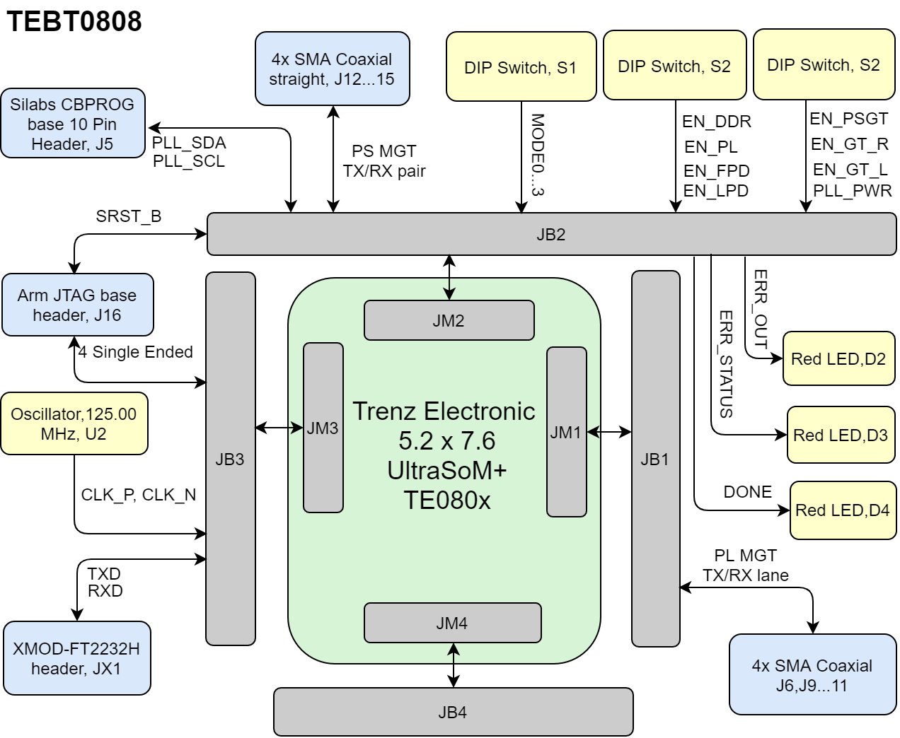 Image Added Image Added
|
|
Main Components
| Page properties |
|---|
|
Notes : |
| Page properties |
|---|
|
Notes : - Picture of the PCB (top and bottom side) with labels of important components
- Add List below
|
...
| Scroll Title |
|---|
| anchor | Figure_OV_BD |
|---|
| title | TExxxx main componentsTEBT0808 Main Components |
|---|
|
| Scroll Ignore |
|---|
| draw.io Diagram |
|---|
| border | truefalse |
|---|
| viewerToolbar | true |
|---|
| |
|---|
| fitWindow | false |
|---|
| diagramDisplayName | |
|---|
| lbox | true |
|---|
| revision | 4 |
|---|
| diagramName | TEBT0808_OV_MC |
|---|
| simpleViewer | false |
|---|
| width | |
|---|
| links | auto |
|---|
| tbstyle | hidden |
|---|
| diagramWidth | 640 |
|---|
| revision | 2 |
|---|
|
|
| Scroll Only |
|---|
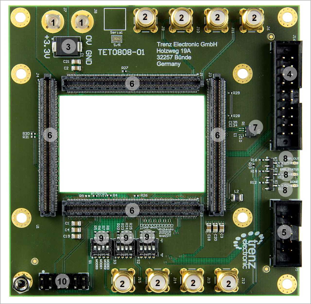 Image Modified Image Modified
|
|
- Uninsulated Power Jack. J7-J8
- SMA Coaxial straight. J6- J9...15
- Surface Mount Schottky Barrier Rectifier. D1
- ARM PJTAG Pin Header J16
- I2C Pin Header, J5
- Board to Board Connectors. J1...4
- MEMS Oscillator, U2
- On-Board LEDs, D2...4
- DIP-Switch, S1...3
- XMOD header, JX1
Initial Delivery State
| Page properties |
|---|
|
Notes : Only components like EEPROM, QSPI flash and DDR3 can be initialized by default at manufacture. If there is no components which might have initial data ( possible on carrier) you must keep the table empty |
...
| Scroll Title |
|---|
| anchor | Table_OV_IDS |
|---|
| title | Initial delivery state of programmable devices on the module |
|---|
|
| Scroll Table Layout |
|---|
| orientation | portrait |
|---|
| sortDirection | ASC |
|---|
| repeatTableHeaders | default |
|---|
| style | |
|---|
| widths | |
|---|
| sortByColumn | 1 |
|---|
| sortEnabled | false |
|---|
| cellHighlighting | true |
|---|
|
Storage device name | Content | Notes |
|---|
Quad SPI Flash- | EEPROM | DDR3 SDRAM | System Controller CPLD- | - |
|
Configuration Signals
| Page properties |
|---|
|
- Overview of Boot Mode, Reset, Enables.
|
Boot mode can be set by DIP-Switch S1.
| Scroll Title |
|---|
| anchor | Table_OV_BP |
|---|
| title | Boot processProcess. |
|---|
|
| Scroll Table Layout |
|---|
| orientation | portrait |
|---|
| sortDirection | ASC |
|---|
| repeatTableHeaders | default |
|---|
| style | |
|---|
| widths | |
|---|
| sortByColumn | 1 |
|---|
| sortEnabled | false |
|---|
| cellHighlighting | true |
|---|
|
|
MODE Signal State | Boot Mode |
|---|
| Scroll Title |
|---|
| anchor | Table_OV_RST |
|---|
| title | Reset process. |
|---|
|
| Scroll Table Layout |
|---|
| orientation | portrait |
|---|
| sortDirection | ASC |
|---|
| repeatTableHeaders | default |
|---|
style | widths | | sortByColumn | 1 |
|---|
| sortEnabled | false |
|---|
| cellHighlighting | true |
|---|
Signal | B2B | I/O | Note |
|---|
Signals, Interfaces and Pins
| Page properties |
|---|
|
Notes : - For carrier or stand-alone boards use subsection for every connector type (add designator on description, not on the subsection title), for example:
- For modules which needs carrier use only classes and refer to B2B connector if more than one is used, for example
|
Board to Board (B2B) I/Os
FPGA bank number and number of I/O signals connected to the B2B connector:
...
| anchor | Table_SIP_B2B |
|---|
| title | General PL I/O to B2B connectors information |
|---|
...
| M3 | M2 | M1 | M0 | Bootmode | Bootmode | Notes |
|---|
| ON | ON | ON | ON | 0b0000 | PS Main JTAG (TE0790 USB JTAG) | DIPs are inverted | | ON | ON | OFF | ON | 0b0010 | SPI Flash (dual parallel, 4bit x 2, 32bit Addressing) | DIPs are inverted | | OFF | ON | ON | ON | 0b1000 | PJTAG(MIO29:26) | DIPs are inverted |
|
| Scroll Title |
|---|
| anchor | Table_OV_RST |
|---|
| title | Reset Process. |
|---|
|
| Scroll Table Layout |
|---|
| orientation | portrait |
|---|
| sortDirection | ASC |
|---|
| repeatTableHeaders | default |
|---|
| style | |
|---|
| widths | |
|---|
| sortByColumn | 1 |
|---|
| sortEnabled | false |
|---|
| cellHighlighting | true |
|---|
|
Signal | B2B | Note |
|---|
PLL_RST | J2-89 |
| | SRST_B | J2-96 | Connected to PJTAG0_SRST - J16 |
|
Signals, Interfaces and Pins
| Page properties |
|---|
|
Notes : - For carrier or stand-alone boards use subsection for every connector type (add designator on description, not on the subsection title), for example:
- For modules which needs carrier use only classes and refer to B2B connector if more than one is used, for example
|
Board to Board (B2B) I/Os
TEBT0808 has four B2B Connectors and each connector has 160 pins. Number of I/O signals and Interfaces connected to the B2B connectors is as following table:
...
JTAG access to the TExxxx SoM through B2B connector JMX.
| Scroll Title |
|---|
| anchor | Table_SIP_JTGB2B |
|---|
| title | JTAG pins connectionGeneral PL I/O to B2B connectors information |
|---|
|
| Scroll Table Layout |
|---|
| orientation | portrait |
|---|
| sortDirection | ASC |
|---|
| repeatTableHeaders | default |
|---|
| style | |
|---|
| widths | |
|---|
| sortByColumn | 1 |
|---|
| sortEnabled | false |
|---|
| cellHighlighting | true |
|---|
|
|
JTAG Signal | B2B Connector |
|---|
TMS | TDI | TDO | TCK | JTAG_EN |
MIO Pins
...
you must fill the table below with group of MIOs which are connected to a specific components or peripherals, you do not have to specify pins in B2B, Just mention which B2B is connected to MIOs. The rest is clear in the Schematic.
Example:
| B2B Connector | Interfaces | Number of I/O | Notes |
|---|
J1
| User I/O | 46 Single Ended, 23 Differential 16 Single Ended, 8 Differential 16 Single Ended, 8 Differential 16 Single Ended, 8 Differential 4 Single Ended | IOs are Loop-Back IOs are Loop-Back IOs are Loop-Back IOs are Loop-Back PL_1V8 | J2
| User IO | 28 Single Ended, 14 Differential 6 Single Ended, 3 Differential | IOs are Loop-Back IOs are Loop-Back | | Boot Mode | 4 Single Ended | MODE0...3 | | Control Signals | 25 Single Ended | PLL_SEL0, PLL_SEL1, PLL_RST, EN_GTR, EN_PL, PLL_LOLN, EN_PSGT, ERR_STATUS, ERR_OUT,SRST_B, INIT_B, PROG_B, EN_FPD , EN_LPD , DONE, EN_PLL_PWR, PLL_FINC ,PG_PLL_1V8, LP_GOOD, PG_DDR, PG_PL, PG_FPD, PG_PSGT, PG_GT_R, PG_GT_L | | JTAG Interface | 7 Single Ended | TCK, TDI, TMS, TDO, MR, Rxd, Txd | | I2C | 2 Single Ended | PLL_SCL, PLL_SDA | | Clock | 6 Single Ended, 3 Differential | CLK0, CLK7, CLK8 | J3
| User IO | 24 Single Ended, 12 Differential 24 Single Ended, 12 Differential | Connected to Module FPGA, Bank 48 Connected to Module FPGA, Bank 47 | | Clock | 6 Single Ended, 3 Differential | CLK228, CLK229, CLK230 | | PJTAG Interface | 4 Single Ended | PJTAG0_TCK, PJTAG0_TDI, PJTAG0_TMS, PJTAG0_TDO, | | MIO | 45 Single Ended | MIO13..77 | | UART | 2 Single Ended | TXD, RXD | | Power Control Signals | 4 Single Ended | PS_1V8, SI_PLL_1V8, VCCO_48, VCCO_47, PLL_3V3 | | J4 | User I/O | 48 Single Ended, 24 Differential 48 Single Ended, 24 Differential 4 Single Ended 4 Single Ended | IOs are Loop-Back IOs are Loop-Back B64_T0...3 B65_T0...3 | | Power pins | 4 Single Ended | VCCO_64, VCCO65 |
|
SMA Coaxial Connectors
TEBT0808 is equipped with 8 SMD Coaxial Connectors.
| Scroll Title |
|---|
| anchor | Table_SIP_SMDCoax |
|---|
| title | SMD Coaxial Connectors |
|---|
|
| Scroll Table Layout |
|---|
| orientation | portrait |
|---|
| sortDirection | ASC |
|---|
| repeatTableHeaders | default |
|---|
| style | |
|---|
| widths | |
|---|
| sortByColumn | 1 |
|---|
| sortEnabled | false |
|---|
| cellHighlighting | true |
|---|
|
| Designator | Schematic | B2B Connector | Notes |
|---|
| J6 | B230_TX3_P | J1 |
| | J9 | B230_RX3_N | J1 |
| | J10 | B230_RX3_P | J1 |
| | J11 | B230_TX3_P | J1 | | J12 | B505_TX0_N | J2 |
| | J13 | B5050TX0_P | J2 |
| | J14 | B505_RX0_N | J2 |
| | J15 | B505_RX0_P | J2 |
|
|
XMOD JTAG
JTAG access to the TEBT080X is available through B2B connector JB2 using XMOD adapter TE0790.
| Scroll Title |
|---|
| anchor | Table_SIP_JTG |
|---|
| title | JTAG Pins Connection |
|---|
|
| Scroll Table Layout |
|---|
| orientation | portrait |
|---|
| sortDirection | ASC |
|---|
| repeatTableHeaders | default |
|---|
| style | |
|---|
| widths | |
|---|
| sortByColumn | 1 |
|---|
| sortEnabled | false |
|---|
| cellHighlighting | true |
|---|
|
JTAG Signal | B2B Connector | Notes |
|---|
| TMS | J2- 126 |
| | TDI | J2- 122 |
| | TDO | J2- 124 |
| | TCK | J2- 120 |
|
|
The voltages 3.3V (VCC) and VIO (variable SC CPLD I/O-voltage) on TE0790 can be configured by the DIP-switch S2 which must be set as following.
| Scroll Title |
|---|
| anchor | Table_SIP_Xmod_DIP |
|---|
| title | Xmod Adapter DIP-Switch Setting Description |
|---|
|
| Scroll Table Layout |
|---|
| orientation | portrait |
|---|
| sortDirection | ASC |
|---|
| repeatTableHeaders | default |
|---|
| style | |
|---|
| widths | |
|---|
| sortByColumn | 1 |
|---|
| sortEnabled | false |
|---|
| cellHighlighting | true |
|---|
|
| DIP Switch,S2 | Default | Description |
|---|
| 1 | ON | Update Mode JTAG access to SC CPLD only | | 2 | OFF | Must be always in OFF state. | | 3 | OFF | VIO is supplied from Module | | 4 | OFF | 3.3V is supplied by the carrier TEBT0808 |
|
PJTAG
PJTAG access to the TEBT0808 is available through B2B connector JB3.
| Scroll Title |
|---|
| anchor | Table_SIP_JTG |
|---|
| title | PJTAG Pins Connection |
|---|
|
| Scroll Table Layout |
|---|
| orientation | portrait |
|---|
| sortDirection | ASC |
|---|
| repeatTableHeaders | default |
|---|
| style | |
|---|
| widths | |
|---|
| sortByColumn | 1 |
|---|
| sortEnabled | false |
|---|
| cellHighlighting | true |
|---|
|
JTAG Signal | B2B Connector | Notes |
|---|
| PJTAG_TMS | J3- 94 |
| | PJTAG_TDI | J3- 90 |
| | PJTAG_TDO | J3- 92 |
| | PJTAG_TCK | J3- 88 |
| | PJTAG_SRST | J2- 96 | Connected to SRST_B |
|
The I2C signals can be accessed through pin header J5.
| Scroll Title |
|---|
| anchor | Table_SIP_I2C |
|---|
| title | I2C Connections |
|---|
|
| Scroll Table Layout |
|---|
| orientation | portrait |
|---|
| sortDirection | ASC |
|---|
| repeatTableHeaders | default |
|---|
| style | |
|---|
| widths | |
|---|
| sortByColumn | 1 |
|---|
| sortEnabled | false |
|---|
| cellHighlighting | true |
|---|
|
Signals | B2B Connector | Pin Header | Notes |
|---|
| PLL_SCL | J2- 90 | J5- 3 |
| | PLL_SDA | J2- 92 | J5- 7 |
|
|
Test Points
| Scroll Title |
|---|
| anchor | Table_SIP_TestPoint |
|---|
| title | Test Points Information |
|---|
|
| Scroll Table Layout |
|---|
| orientation | portrait |
|---|
| sortDirection | ASC |
|---|
| repeatTableHeaders | default |
|---|
| style | |
|---|
| widths | |
|---|
| sortByColumn | 1 |
|---|
| sortEnabled | false |
|---|
| cellHighlighting | true |
|---|
|
Test Point | Signals | B2B Connector | Notes |
|---|
| TP 1 | DDR_1V2 | J2-135 |
| | TP 2 | PG_PSGT | J2-82 |
| | TP 3 | ERR_STATUS | J2-86 |
| | TP 4 | PLL_FDEC | J2-94 |
| | TP 5 | EN_LPD | J2-108 |
| | TP 6 | EN_DDR | J2-112 |
| | TP 7 | PG_PL | J2-104 |
| | TP 8 | PG_PLL_1V8 | J2-80 |
| | TP 9 | N_PSGT | J2-84 |
| | TP 10 | ERR_OUT | J2-88 |
| | TP 11 | EN_FPD | J2-102 |
| | TP 12 | LP_GOOD | J2-106 |
| | TP 13 | PG_FPD | J2-110 |
| | TP 14 | PG_DDR | J2-114 |
| | TP 15 | EN_PLL_PWR | J2-77 |
| | TP 16 | PLL_FINC | J2-81 |
| | TP 17 | PG_GT_R | J2-91 |
| | TP 18 | EN_GT_R | J2-95 |
| | TP 19 | EN_PL | J2-101 |
| | TP 20 | EN_GT_L | J2-79 |
| | TP 21 | PLL_SEL0 | J2-93 |
| | TP 22 | PG_GT_L | J2-97 |
| | TP 23 | INIT_B | J2-98 |
| | TP 24 | IN1_P | J2-4 |
| | TP 25 | PLL_SEL1 | J2-87 |
| | TP 26 | PLL_LOLN | J2-85 |
| | TP 27 | PLL_RST | J2-89 |
| | TP 28 | DX_P | J2-119 |
| | TP 29 | DX_N | J2-121 |
| | TP 30 | IN1_N | J2-6 |
| | TP 31 | B505_CLK0_P | J2-10 |
| | TP 32 | B505_CLK0_N | J2-12 |
| | TP 33 | B505_CLK1_P | J2-16 |
| | TP 34 | B505_CLK1_N | J2-18 |
| | TP 35 | B128_CLK1_P | J2-22 |
| | TP 36 | B128_CLK1_N | J2-24 |
| | TP 37 | CLK0_N | J2-1 |
| | TP 38 | CLK0_P | J2-3 |
| | TP 39 | CLK8_P | J2-7 |
| | TP 40 | CLK8_N | J2-9 |
| | TP 41 | CLK7_P | J2-13 |
| | TP 42 | CLK7_N | J2-15 |
| | TP 43 | IN2_P | J3-66 |
| | TP 44 | IN2_N | J3-68 |
| | TP 45 | B230_CLK1_N | J3-59 |
| | TP 46 | B230_CLK1_P | J3-61 |
| | TP 47 | B229_CLK0_N | J3-65 |
| | TP 48 | B229_CLK0_P | J3-67 |
| | TP 49 | PLL_3V3 | J3-152 |
| | TP 50 | GND | J3-155 |
| | TP 51 | PL_1V8 | J1-121 |
| | TP 52 | PS_1V8 | J3-147 |
| | TP 53 | SI_PLL_1V8 | J3-151 |
| | TP 54 | PROG_B | J2-100 |
| | TP 55...56 | GND | - |
|
|
On-board Peripherals
| Page properties |
|---|
|
Notes : - add subsection for every component which is important for design, for example:
- Two 100 Mbit Ethernet Transciever PHY
- USB PHY
- Programmable Clock Generator
- Oscillators
- eMMCs
- RTC
- FTDI
- ...
- DIP-Switches
- Buttons
- LEDs
|
| Page properties |
|---|
|
Notes : In the on-board peripheral table "chip/Interface" must be linked to the corresponding chapter or subsection |
| Scroll Title |
|---|
| anchor | Table_OBP |
|---|
| title | On Board Peripherals |
|---|
|
| Scroll Table Layout |
|---|
| orientation | portrait |
|---|
| sortDirection | ASC |
|---|
| repeatTableHeaders | default |
|---|
| style | |
|---|
| widths | |
|---|
| sortByColumn | 1 |
|---|
| sortEnabled | false |
|---|
| cellHighlighting | true |
|---|
|
|
DIP Switch
There are three DIP Switches, S1, S2, S3.
The Boot Mode can be set through DIP Switch S1, refer to BootMode table.
| Scroll Title |
|---|
| anchor | Table_OBP_DIP |
|---|
| title | DIP Switch S1 |
|---|
|
...
SPI_CS , SPI_DQ0... SPI_DQ3
SPI_SCK
...
| anchor | Table_OBP_MIOs |
|---|
| title | MIOs pins |
|---|
...
| Page properties |
|---|
|
Notes : - add subsection for every component which is important for design, for example:
- Two 100 Mbit Ethernet Transciever PHY
- USB PHY
- Programmable Clock Generator
- Oscillators
- eMMCs
- RTC
- FTDI
- ...
- DIP-Switches
- Buttons
- LEDs
|
| Page properties |
|---|
|
Notes : In the on-board peripheral table "chip/Interface" must be linked to the corresponding chapter or subsection |
| Scroll Title |
|---|
| anchor | Table_OBP |
|---|
| title | On board peripherals |
|---|
|
| Scroll Table Layout |
|---|
| orientation | portrait |
|---|
| sortDirection | ASC |
|---|
| repeatTableHeaders | default |
|---|
| style | |
|---|
| widths | |
|---|
| sortByColumn | 1 |
|---|
| sortEnabled | false |
|---|
| cellHighlighting | true |
|---|
|
|
| Chip/Interface | Designator | Notes |
|---|
Quad SPI Flash Memory
...
Notes :
...
| DIP Switch S1 | Signals | B2B | Notes |
|---|
| S1A | MODE0 | J2-109 |
| | S1B | MODE1 | J2-107 |
| | S1C | MODE2 | J2-105 |
| | S1D | MODE3 | J2-103 |
|
|
Control signals must be set using DIP Switch S2, S3.
| Scroll Title |
|---|
| anchor | Table_OBP_SPIDIP |
|---|
| title | Quad SPI interface MIOs and pinsDIP Switch S2 |
|---|
|
| Scroll Table Layout |
|---|
| orientation | portrait |
|---|
| sortDirection | ASC |
|---|
| repeatTableHeaders | default |
|---|
| style | |
|---|
| widths | |
|---|
| sortByColumn | 1 |
|---|
| sortEnabled | false |
|---|
| cellHighlighting | true |
|---|
|
|
...
| S2A | EN_PSGT | J2-84 | Position OFF enables power rail | | S2B | EN_GT_R | J2-95 | Position OFF enables power rail | | S2C | EN_GT_L | J2-97 | Position OFF enables power rail | | S2D | EN_PLL_PWR | J2-77 | Position OFF enables power rail, connected to PG_PL |
|
| Scroll Title |
|---|
| anchor | Table_OBP_RTC |
|---|
| title | I2C interface MIOs and pins |
|---|
|
| Scroll Table Layout |
|---|
|
| orientation | portrait |
|---|
| sortDirection | ASC |
|---|
| repeatTableHeaders | default |
|---|
style | widths | | sortByColumn | 1 |
|---|
| sortEnabled | false |
|---|
| cellHighlighting | true |
|---|
| MIO Pin | Schematic | U? Pin | Notes |
|---|
| Scroll Title |
|---|
| anchor | Table_OBP_I2C_RTCDIP |
|---|
| title | I2C Address for RTCDIP Switch S3 |
|---|
|
| Scroll Table Layout |
|---|
| orientation | portrait |
|---|
| sortDirection | ASC |
|---|
| repeatTableHeaders | default |
|---|
| style | |
|---|
| widths | |
|---|
| sortByColumn | 1 |
|---|
| sortEnabled | false |
|---|
| cellHighlighting | true |
|---|
|
|
| MIO Pin | I2C Address | Designator | Notes |
|---|
...
| DIP Switch S3 | Signals | B2B | S3 switch | Notes |
|---|
| S3A | EN_DDR | J2-112 | S3A | Position OFF enables power rail | | S3B | EN_LPD | J2-108 | S3B | Position OFF enables power rail | | S3C | EN_PL | J2-101 | S3C | Position OFF enables power rail | | S3D | EN_FPD | J2-102 | S3D | Position OFF enables power rail |
|
LEDs
| Scroll Title |
|---|
| anchor | Table_OBP_EEPLED |
|---|
| title | I2C EEPROM interface MIOs and pinsOn-board LEDs |
|---|
|
| Scroll Table Layout |
|---|
| orientation | portrait |
|---|
| sortDirection | ASC |
|---|
| repeatTableHeaders | default |
|---|
| style | |
|---|
| widths | |
|---|
| sortByColumn | 1 |
|---|
| sortEnabled | false |
|---|
| cellHighlighting | true |
|---|
|
MIO Pin| Schematic | U?? Pin | Notes | |
| Scroll Title |
|---|
| anchor | Table_OBP_I2C_EEPROM |
|---|
| title | I2C address for EEPROM |
|---|
|
| Scroll Table Layout |
|---|
| orientation | portrait |
|---|
| sortDirection | ASC |
|---|
| repeatTableHeaders | default |
|---|
style | widths | | sortByColumn | 1 |
|---|
| sortEnabled | false |
|---|
| cellHighlighting | true |
|---|
| MIO Pin | I2C Address | Designator | Notes |
|---|
...
| Color | Connected to | Active Level | Note |
|---|
| D2 | Red | DONE | Active High | Non User LED | | D3 | Red | ERR_STATUS | Active High | Non User LED | | D4 | Red | ERR_OUT | Active High | Non User LED |
|
Clock Sources
| Scroll Title |
|---|
| anchor | Table_OBP_LEDCLK |
|---|
| title | On-board LEDsOsillators |
|---|
|
| Scroll Table Layout |
|---|
| orientation | portrait |
|---|
| sortDirection | ASC |
|---|
| repeatTableHeaders | default |
|---|
| style | |
|---|
| widths | |
|---|
| sortByColumn | 1 |
|---|
| sortEnabled | false |
|---|
| cellHighlighting | true |
|---|
|
|
| Schematic | Color | Connected to | Active Level | Note |
|---|
...
| Designator | Description | Frequency | Note |
|---|
| U2 | MEMS Oscillator | 125.00 MHz |
|
|
Power and Power-On Sequence
| Page properties |
|---|
|
Notes : Minimum and Maximum density of DDR3 SDRAM must be mentioned for other assembly options. (pay attention to supported address length for DDR3) |
The TE???? SoM has ??? GByte volatile DDR3 SDRAM IC for storing user application code and data.
- Part number:
- Supply voltage:
- Speed:
- NOR Flash
- Temperature:
...
In 'Power and Power-on Sequence' section there are three important digrams which must be drawn: - Power on-sequence
- Power distribution
- Voltage monitoring circuit
|
Power Supply
| Scroll Title |
|---|
| anchor | Table_OBPPWR_ETHPC |
|---|
| title | Ethernet PHY to Zynq SoC connectionsPower Consumption |
|---|
|
| Scroll Table Layout |
|---|
| orientation | portrait |
|---|
| sortDirection | ASC |
|---|
| repeatTableHeaders | default |
|---|
| style | |
|---|
| widths | |
|---|
| sortByColumn | 1 |
|---|
| sortEnabled | false |
|---|
| cellHighlighting | true |
|---|
|
|
| Bank | Signal Name | ETH1 | ETH2 | Signal Description |
|---|
...
| 2,0mm MC LB2 | Note |
|---|
| J7 | 3.3V direct modules power supply | | J8 | GND |
|
Power Consumption
Minimum current depends mainly on design and cooling solution. Use Xilinx Power Estimator and/or Your Vivado Project to estimate min current. Minimum of 3A are recommanded for basic functionality.
| Scroll Title |
|---|
| anchor | Table_OBPPWR_CANPC |
|---|
| title | CAN Tranciever interface MIOsPower Consumption |
|---|
|
| Scroll Table Layout |
|---|
| orientation | portrait |
|---|
| sortDirection | ASC |
|---|
| repeatTableHeaders | default |
|---|
| style | |
|---|
| widths | |
|---|
| sortByColumn | 1 |
|---|
| sortEnabled | false |
|---|
| cellHighlighting | true |
|---|
|
| Bank | Schematic | U?? Notes | D-Tx | Driver Input | R-Rx | Reciever Output | |
...
* TBD - To Be Determined
Power Distribution Dependencies
Input oower sourced directly the module, Only one Diode D1 is used for inverse polarity protection.
| Scroll Title |
|---|
| anchor | TableFigure_OBPPWR_CLKPD |
|---|
| title | OsillatorsPower Distribution |
|---|
|
tablelayout |
| orientation | portrait |
|---|
| sortDirection | ASC |
|---|
| repeatTableHeaders | default |
|---|
style | widths | | sortByColumn | 1 |
|---|
sortEnabledcellHighlightingDesignatorDescriptionFrequencyNoteMHzMHz | KHz |
Power and Power-On Sequence
...
In 'Power and Power-on Sequence' section there are three important digrams which must be drawn:
- Power on-sequence
- Power distribution
- Voltage monitoring circuit
| Note |
|---|
For more information regarding how to draw diagram, Please refer to "Diagram Drawing Guidline" . |
| revision | 4 |
|---|
| diagramName | TEBT0808_PWR_PD |
|---|
| simpleViewer | false |
|---|
| width | |
|---|
| links | auto |
|---|
| tbstyle | hidden |
|---|
| diagramWidth | 640 |
|---|
|
|
| Scroll Only |
|---|
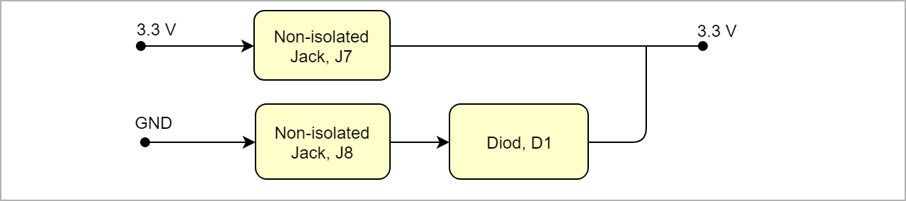 Image Added Image Added
|
|
Power Rails
Power Supply
Power supply with minimum current capability of xx A for system startup is recommended.
...
| Scroll Title |
|---|
| anchor | Table_PWR_PC |
|---|
| title | Power Consumption |
|---|
| | Scroll Table Layout |
|---|
| orientation | portrait |
|---|
| sortDirection | ASC |
|---|
| repeatTableHeaders | default |
|---|
style | widths | | sortByColumn | 1 |
|---|
| sortEnabled | false |
|---|
| cellHighlighting | true |
|---|
| Power Input Pin | Typical Current |
|---|
| VIN | TBD* |
* TBD - To Be Determined
Power Distribution Dependencies
...
| anchor | Figure_PWR_PD |
|---|
| title | Power Distribution |
|---|
| Scroll Ignore |
|---|
Create DrawIO object here: Attention if you copy from other page, objects are only linked. |
| Scroll Only |
|---|
image link to the generate DrawIO PNG file of this page. This is a workaround until scroll pdf export bug is fixed |
| PR | | title | Module power rails. |
|---|
|
| Scroll Table Layout |
|---|
| orientation | portrait |
|---|
| sortDirection | ASC |
|---|
| repeatTableHeaders | default |
|---|
| style | |
|---|
| widths | |
|---|
| sortByColumn | 1 |
|---|
| sortEnabled | false |
|---|
| cellHighlighting | true |
|---|
|
Power Rail Name | B2B J1 Pins | B2B J2 Pins | B2B J3 Pins | Directions | Note |
|---|
| PL_DCIN | 151, 153, 155, 157, 159 | - | - | Output | - | | DCDCIN | - | 154, 156, 158, 160,
153, 155, 157, 159 | - | Output | - | | LP_DCDC | - | 138, 140, 142, 144 | - | Output | - | | PS_BATT | - | 125 | - | Output | - | | GT_DCDC | - | - | 157, 158, 159, 160 | Output | - | | PLL_3V3 | - | - | 152 | Output | - | | SI_PLL_1V8 | - | - | 151 | Input | - | | PS_1V8 | - | 99 | 147, 148 | Input | - | | PL_1V8 | 91, 121 | - | - | Input | - | | DDR_1V2 | - | 135 | - | Input | - |
|
Board to Board Connectors
| Page properties |
|---|
|
- This section is optional and only for modules.
use "include page" macro and link to the general B2B connector page of the module series, For example: 6 x 6 SoM LSHM B2B Connectors
| Include Page |
|---|
| 6 x 6 SoM LSHM B2B Connectors |
|---|
| 6 x 6 SoM LSHM B2B Connectors |
|---|
|
|
| Include Page |
|---|
| 5.2 x 7.6 UltraSoM+ ST5 and SS5 B2B Connectors |
|---|
| 5.2 x 7.6 UltraSoM+ ST5 and SS5 B2B Connectors |
|---|
|
Technical Specifications
Absolute Maximum Ratings
Power-On Sequence
...
| anchor | Figure_PWR_PS |
|---|
| title | Power Sequency |
|---|
| Scroll Ignore |
|---|
Create DrawIO object here: Attention if you copy from other page, objects are only linked. |
| Scroll Only |
|---|
image link to the generate DrawIO PNG file of this page. This is a workaround until scroll pdf export bug is fixed |
Voltage Monitor Circuit
...
| anchor | Figure_PWR_VMC |
|---|
| title | Voltage Monitor Circuit |
|---|
| Scroll Ignore |
|---|
Create DrawIO object here: Attention if you copy from other page, objects are only linked. |
| Scroll Only |
|---|
image link to the generate DrawIO PNG file of this page. This is a workaround until scroll pdf export bug is fixed |
Power Rails
...
| anchor | Table_PWR_PR |
|---|
| title | Module power rails. |
|---|
...
B2B Connector
JM1 Pin
...
B2B Connector
JM2 Pin
...
B2B Connector
JM3 Pin
...
Bank Voltages
| Scroll Title |
|---|
| anchor | Table_PWRTS_BVAMR |
|---|
| title | Zynq SoC bank voltages.PS absolute maximum ratings |
|---|
|
| Scroll Table Layout |
|---|
| orientation | portrait |
|---|
| sortDirection | ASC |
|---|
| repeatTableHeaders | default |
|---|
| style | |
|---|
| widths | |
|---|
| sortByColumn | 1 |
|---|
| sortEnabled | false |
|---|
| cellHighlighting | true |
|---|
|
| Schematic Name | | Notes |
|---|
|
...
...
| Symbols | Min | Max | Unit | Note |
|---|
| VIN | -0.3 | 4 | V | VIN is connected directly to module | | Storage Temperatur | -40 | +85 | °C | See DIP Switch, CHS-04TA datasheet |
|
Recommended Operating Conditions
Operating temperature range depends also on customer design and cooling solution. Please contact us for options.
use "include page" macro and link to the general B2B connector page of the module series,
...
? x ? modules use two or three Samtec Micro Tiger Eye Connector on the bottom side.
3 x REF-??????? (compatible to ????????), (?? pins, ?? per row)
Operating Temperature: -??°C ~ ??°C
Current Rating: ??A per ContactNumber of Positions: ??
Number of Rows: ??
Technical Specifications
...
| Scroll Title |
|---|
| anchor | Table_TS_AMR |
|---|
| title | PS absolute maximum ratings |
|---|
| | Scroll Table Layout |
|---|
| orientation | portrait |
|---|
| sortDirection | ASC |
|---|
| repeatTableHeaders | default |
|---|
style | widths | | sortByColumn | 1 |
|---|
| sortEnabled | false |
|---|
| cellHighlighting | true |
|---|
| Symbols | Description | Min | Max | Unit |
|---|
V | V | V | V | V | V | V | V |
Recommended Operating Conditions
...
| ROC | | title | Recommended operating conditions. |
|---|
|
| Scroll Table Layout |
|---|
| orientation | portrait |
|---|
| sortDirection | ASC |
|---|
| repeatTableHeaders | default |
|---|
| style | |
|---|
| widths | |
|---|
| sortByColumn | 1 |
|---|
| sortEnabled | false |
|---|
| cellHighlighting | true |
|---|
|
| Symbols | Min | Max | Unit | Note |
|---|
| VIN | 3,14 | 3.47 | V | Check also TRM of the connected module | | Operating Temperatur | -40 | +85 | °C |
|
|
Physical Dimensions
Module size: 90 mm × 90 mm. Please download the assembly diagram for exact numbers.
Mating height with standard connectors: 3.5 mm.
PCB thickness: 1.6 mm.
| Page properties |
|---|
|
In 'Physical Dimension' section, top and button view of moduloe must be insterted, information regarding physical dimention can be obtained through webpage for product in Shop.Trenz, (Download> Documents> Assembly part)for every SoM. For Example: for Module TE0728, Physical Dimension information can be captured by snipping tools from the link below: https://www.trenz-electronic.de/fileadmin/docs/Trenz_Electronic/Modules_and_Module_Carriers/5.2x7.6/TE0745/REV02/Documents/AD-TE0745-02-30-1I.PDF
|
| Scroll Title |
|---|
| anchor | TableFigure_TS_ROCPD |
|---|
| title | Recommended operating conditions.Physical Dimension |
|---|
|
tablelayoutorientationportraitsortDirectionASCrepeatTableHeadersdefaultstylewidthssortByColumn1sortEnabledfalse |
| cellHighlighting | true |
|---|
| Parameter | Min | Max | Units | Reference Document |
|---|
V | See ???? datasheets. | V | See Xilinx ???? datasheet. | V | See Xilinx ???? datasheet. | V | See Xilinx ???? datasheet. | V | See Xilinx ???? datasheet. | V | See Xilinx ???? datasheet. | V | See Xilinx ???? datasheet. | °C | See Xilinx ???? datasheet. | °C | See Xilinx ???? datasheet. |
Physical Dimensions
Module size: ?? mm × ?? mm. Please download the assembly diagram for exact numbers.
Mating height with standard connectors: ? mm.
...
| diagramName | TEBT0808_PS_PD |
|---|
| simpleViewer | false |
|---|
| width | |
|---|
| links | auto |
|---|
| tbstyle | hidden |
|---|
| diagramWidth | 641 |
|---|
|
|
| Scroll Only |
|---|
| scroll-pdf | true |
|---|
| scroll-office | true |
|---|
| scroll-chm | true |
|---|
| scroll-docbook | true |
|---|
| scroll-eclipsehelp | true |
|---|
| scroll-epub | true |
|---|
| scroll-html | true |
|---|
| 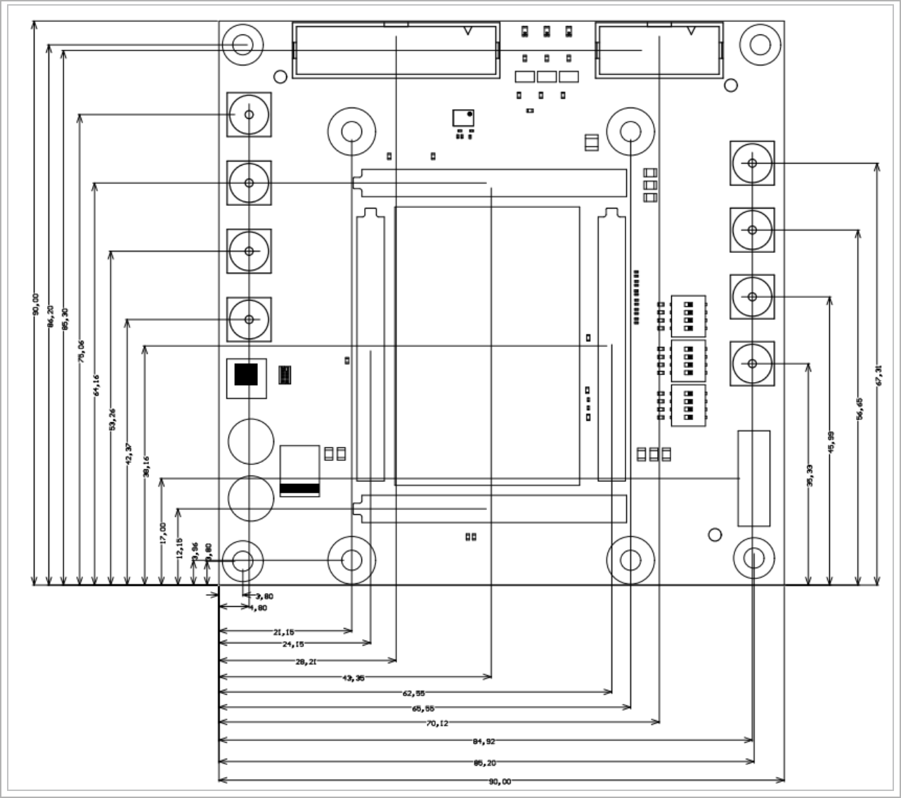 Image Added Image Added
|
|
Currently Offered Variants
| Page properties |
|---|
|
Set correct link to the shop page overview table of the product on English and German. Example for TE0728: ENG Page: https://shop.trenz-electronic.de/en/Products/Trenz-Electronic/TE07XX-Zynq-SoC/TE0728-Zynq-SoC/ DEU Page: https://shop.trenz-electronic.de/de/Produkte/Trenz-Electronic/TE07XX-Zynq-SoC/TE0728-Zynq-SoC/ if not available, set. In 'Physical Dimension' section, top and button view of moduloe must be insterted, information regarding physical dimention can be obtained through webpage for product in Shop.Trenz, (Download> Documents> Assembly part)for every SoM. For Example: for Module TE0728, Physical Dimension information can be captured by snipping tools from the link below: https://wwwfileadmindocs_Modules_and_Module_Carriers/5.2x7.6/TE0745/REV02/Documents/AD-TE0745-02-30-1I.PDF| Note |
|---|
For more information regarding how to draw diagram, Please refer to "Diagram Drawing Guidline" . |
| Scroll Title |
|---|
| anchor | FigureTable_TSVCP_PDSO |
|---|
| title | Physical DimensionTrenz Electronic Shop Overview |
|---|
|
| ignore |
Create DrawIO object here: Attention if you copy from other page, objects are only linked. |
| Scroll Only |
|---|
| scroll-pdf | true |
|---|
| scroll-office | true |
|---|
| scroll-chm | true |
|---|
| scroll-docbook | true |
|---|
| scroll-eclipsehelp | true |
|---|
| scroll-epub | true |
|---|
| scroll-html | true |
|---|
|
image link to the generate DrawIO PNG file of this page. This is a workaround until scroll pdf export bug is fixed |
Currently Offered Variants
...
Set correct link to the shop page overview table of the product on English and German.
Example for TE0728:
ENG Page: https://shop.trenz-electronic.de/en/Products/Trenz-Electronic/TE07XX-Zynq-SoC/TE0728-Zynq-SoC/
DEU Page: https://shop.trenz-electronic.de/de/Produkte/Trenz-Electronic/TE07XX-Zynq-SoC/TE0728-Zynq-SoC/
if not available, set.
| tablelayout |
|---|
| orientation | portrait |
|---|
| sortDirection | ASC |
|---|
| repeatTableHeaders | default |
|---|
| style | |
|---|
| widths | |
|---|
| sortByColumn | 1 |
|---|
| sortEnabled | false |
|---|
| cellHighlighting | true |
|---|
|
|
Revision History
Hardware Revision History
| Scroll Title |
|---|
| anchor | Table_RH_HRH |
|---|
| title | Hardware Revision History |
|---|
|
| Scroll Table Layout |
|---|
| orientation | portrait |
|---|
| sortDirection | ASC |
|---|
| repeatTableHeaders | default |
|---|
| style | |
|---|
| widths | |
|---|
| sortByColumn | 1 |
|---|
| sortEnabled | false |
|---|
| cellHighlighting | true |
|---|
|
| Date | Revision | Changes | Documentation Link |
|---|
| 2016-05-30 | 01 | Initial Release | REV01 |
|
Hardware revision number can be found on the PCB board together with the module model number separated by the dash.
...
https://shop.trenz-electronic.de/de/Produkte/Trenz-Electronic/
...
| Scroll Title |
|---|
| anchor | TableFigure_VCPRV_SOHRN |
|---|
| title | Trenz Electronic Shop Overview Board hardware revision number. |
|---|
|
tablelayout |
| orientation | portrait |
|---|
| sortDirection | ASC |
|---|
| repeatTableHeaders | default |
|---|
style | widths | | sortByColumn | 1 |
|---|
sortEnabledcellHighlighting| Trenz shop TE0728 overview page |
|---|
| English page | German page |
Revision History
Hardware Revision History
| | |
|---|
| fitWindow | false |
|---|
| diagramDisplayName | |
|---|
| lbox | true |
|---|
| revision | 1 |
|---|
| diagramName | TEBT0808_RV_HRN |
|---|
| simpleViewer | false |
|---|
| width | |
|---|
| links | auto |
|---|
| tbstyle | hidden |
|---|
| diagramWidth | 158 |
|---|
|
|
| Scroll Only |
|---|
| scroll-pdf | true |
|---|
| scroll-office | true |
|---|
| scroll-chm | true |
|---|
| scroll-docbook | true |
|---|
| scroll-eclipsehelp | true |
|---|
| scroll-epub | true |
|---|
| scroll-html | true |
|---|
| 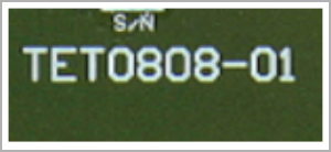 Image Added Image Added
|
|
| Scroll Title |
|---|
| anchor | Table_RH_HRH |
|---|
| title | Hardware Revision History |
|---|
|
| Scroll Table Layout |
|---|
|
| orientation | portrait |
|---|
| sortDirection | ASC |
|---|
| repeatTableHeaders | default |
|---|
style | widths | | sortByColumn | 1 |
|---|
| sortEnabled | false |
|---|
| cellHighlighting | true |
|---|
| Date | Revision | Note | PCN |
|---|
- | -
Document Change History
| Page properties |
|---|
|
- Note this list must be only updated, if the document is online on public doc!
- It's semi automatically, so do following
Add new row below first Copy "Page Information Macro(date)" Macro-Preview, Metadata Version number, Author Name and description to the empty row. Important Revision number must be the same as the Wiki document revision number Update Metadata = "Page Information Macro (current-version)" Preview+1 and add Author and change description. --> this point is will be deleted on newer pdf export template - Metadata is only used of compatibility of older exports
|
...
| Scroll Title |
|---|
| anchor | Table_RH_DCH |
|---|
| title | Document change history. |
|---|
|
| Scroll Table Layout |
|---|
| orientation | portrait |
|---|
| sortDirection | ASC |
|---|
| repeatTableHeaders | default |
|---|
| style | |
|---|
| widths | |
|---|
| sortByColumn | 1 |
|---|
| sortEnabled | false |
|---|
| cellHighlighting | true |
|---|
|
| Date | Revision | Contributor | Description |
|---|
| Page info |
|---|
| infoType | Modified date |
|---|
| dateFormat | yyyy-MM-dd |
|---|
| type | Flat |
|---|
|
| | Page info |
|---|
| infoType | Current version |
|---|
| prefix | v. |
|---|
| type | Flat |
|---|
| showVersions | false |
|---|
|
| | Page info |
|---|
| infoType | Modified by |
|---|
| type | Flat |
|---|
| showVersions | false |
|---|
|
change list | | | 2020-05-11 | v.54 | John Hartfiel | add notes to DIP section - Correction on configuration signal section
| | 2020-01-24 | v.49 | Pedram Babakhani | | -- | all | Edit | Page info |
|---|
| infoType | Modified users |
|---|
| type | Flat |
|---|
| showVersions | false |
|---|
|
| |
|
Disclaimer
| Include Page |
|---|
| IN:Legal Notices |
|---|
| IN:Legal Notices |
|---|
|
...