Page History
...
- MPSoC: ZYNQ UltraScale+ ZU9EG 900 pin package
- Memory
- 64-Bit DDR4, 8 GByte maximum
- Dual SPI boot Flash in parallel, 512 MByte maximum - User I/O
- 65 x MIO, 48 x HD (all), 156 x HP (3 banks)
- Serial transceiver: 4 x GTR + 16 x GTH
- Transceiver clocks inputs and outputs
- PLL clock generator inputs and outputs - Size: 52 x 76 mm, 3 mm mounting holes for skyline heat spreader
- B2B connectors: 4 x 160 pin
- Si5345 - 10 output PLL
- All power supplies on board, single 3.3V power source required
- 14 on-board DCDC regulators and 13 LDOs
- LP, FP, PL separately controlled power domains - Support for all boot modes (except NAND) and scenarios
- Support for any combination of PS connected peripherals
Block Diagram
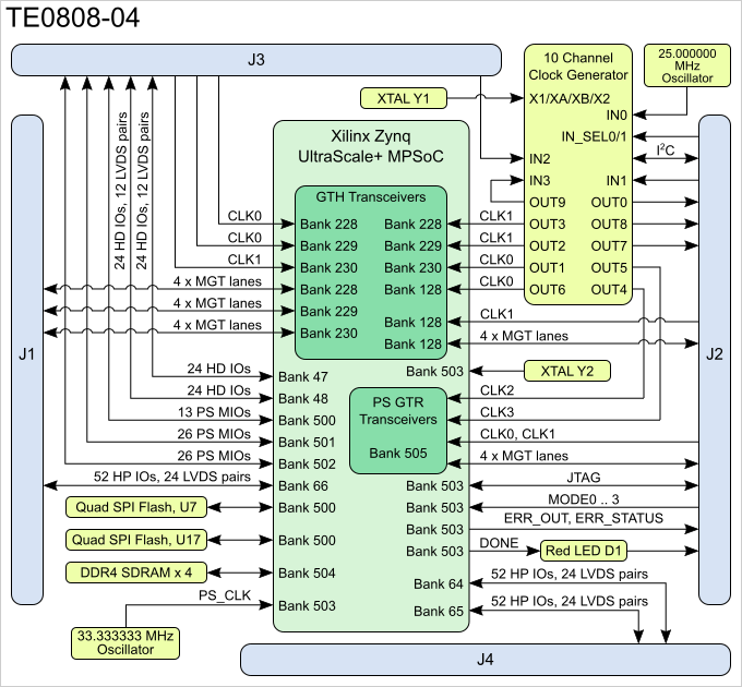
Figure 1: TE0808-04 Block Diagram
...
Table 7: MIO-pin assignment of the Quad SPI Flash memory ICs
Boot Process
The boot source of the Zynq Ultrascale MPSoC can be selected via 4 dedicated pins, which generate a 4-bit code to select the boot mode. The pins are accessible on B2B connector J2:
| Boot Mode Pin | B2B Pin |
|---|---|
| PS_MODE0 | J2-109 |
| PS_MODE1 | J2-107 |
| PS_MODE2 | J2-105 |
| PS_MODE3 | J2-103 |
Table 8: Boot mode pins on B2B connector J2
Following boot modes are possible on the TE0808 Ultrascale module by generating the corresponding 4-bit code by the pins 'PS_MODE0' ... 'PS_MODE3' (little endian alignment):
| Boot Mode | Mode Pins [3:0] | MIO Location | Description |
|---|---|---|---|
| JTAG | 0x0 | JTAG | Dedicated PS interface. |
| QSPI32 | 0x2 | MIO[12:0] | Configured on module with dual QSPI Flash Memory. 32-bit addressing. |
| SD0 | 0x3 | MIO[25:13] | Supports SD 2.0. |
| SD1 | 0x5 | MIO[51:38] | Supports SD 2.0. |
| eMMC_18 | 0x6 | MIO[22:13] | Supports eMMC 4.5 at 1.8V. |
| USB 0 | 0111b | MIO[52:63] | Supports USB 2.0 and USB 3.0. |
| PJTAG_0 | 0x8 | MIO[29:26] | PS JTAG connection 0 option. |
| SD1-LS | 0xE | MIO[51:39] | Supports SD 3.0 with a required |
Table 9: Selectable boot modes by dedicated boot mode pins
Full access to B2B connector. For Functional details see ug1085 - Zynq ultrascale TRM (Boot Modes Section).
...
On-board Peripherals
Flash
...
| Name | IC | Designator | PS7 | MIO | Notes |
|---|---|---|---|---|---|
| SPI Flash | N25Q256A11E1240E | U7 | QSPI0 | MIO0 ... MIO5 | dual parallel booting possible, 32 MByte memory per Flash IC at standard configuration |
| SPI Flash | N25Q256A11E1240E | U17 | QSPI0 | MIO7 ... MIO12 | as above |
Table 810: Peripherals connected to the PS MIO-pins
...
| Input | Connected to | Frequency | Notes |
|---|---|---|---|
| IN0 | On-board Oscillator (U25) | 25.000000 MHz | - |
| IN1 | B2B Connector pins J2-3, J2-1 (differential pair) | User | AC decoupling required on base |
| IN2 | B2B Connector pins J3-66, J3-68 (differential pair) | User | AC decoupling required on base |
| IN3 | OUT9 | User | Loop-back from OUT9 |
| Output | Connected to | Frequency | Notes |
| OUT0 | B2B Connector pins J2-3, J2-1 (differential pair) | User | Default off |
| OUT1 | B230 CLK0 | User | Default off |
| OUT2 | B229 CLK1 | User | Default off |
| OUT3 | B228 CLK1 | User | Default off |
| OUT4 | B505 CLK2 | User | Default off |
| OUT5 | B505 CLK3 | User | Default off |
| OUT6 | B128 CLK0 | User | Default off |
| OUT7 | B2B Connector pins J2-7, J2-9 (differential pair) | User | Default off |
| OUT8 | B2B Connector pins J2-13, J2-15 (differential pair) | User | Default off |
| OUT9 | IN3 (Loop-back) | User | Default off |
| XA/XB | Quartz (Y1) | 50.000 MHz | - |
Table 911: Programmable PLL clock generator input/output
...
| Signal | B2B Connector Pin | Function |
|---|---|---|
| PLL_FINC | J2-81 | Frequency Increment |
| PLL_LOLN | J2-85 | Loss Of Lock (low-active) |
| PLL_SEL0 / PLL_SEL1 | J2-93 / J2-87 | Manual Input Switching |
| PLL_FDEC | J2-94 | Frequency Decrement |
| PLL_RST | J2-59 | Device Reset (low-active) |
| PLL_SCL / PLL_SDA | J2-90 / J2-92 | I²C interface, extern pull-ups needed for SCL- / SDA-line. I²C address in current configuration: 1101000b |
Table 1012: B2B connector pin-out of Si5345A programmable clock generator
...
| Clock | Frequency | Bank 503 Pin | Connected to |
|---|---|---|---|
| PS_CLK | 33.333333 MHz | P20 | MEMS Oscillator, U32 |
| PS_PAD (RTC) | 32.768 kHz | R22/R23 | Quartz crystal, Y2 |
Table 1113: Reference clock-signals to PS configuration bank 503
...
LED | Color | Connected to | Description and Notes |
|---|---|---|---|
| D1 | red | DONE signal (PS Configuration Bank 503) | This LED goes ON when power has been applied to the module and stays ON until MPSoC's programmable logic is configured properly. |
Table 1214: LED's description
Power and Power-On Sequence
...
| Power Input Pin | Typical Current |
|---|---|
| DCDCIN | TBD* |
| LP_DCDC | TBD* |
| PL_DCIN | TBD* |
| PS_BATT | TBD* |
Table 1315: Maximum current of power supplies. *to be determined soon with reference design setup.
...
| Enable-Signal | B2B Connector Pin | Max. Voltage | Note | Power-Good-Signal | B2B Connector Pin | Pull-up Resistor | Note | |
|---|---|---|---|---|---|---|---|---|
| EN_LPD | J2-108 | 6V | TPS82085SIL data sheet | LP_GOOD | J2-106 | 4K7, pulled up to LP_DCDC | - | |
| EN_FPD | J2-102 | DCDCIN | NC7S08P5X data sheet | PG_FPD | J2-110 | 4K7, pulled up to DCDCIN | - | |
| EN_PL | J2-101 | PL_DCIN | left floating for logic high (drive to GND for logic low) | PG_PL | J2-104 | extern pull-up needed (max. voltage 'GT_DCDC'), max. sink current 1 mA | TPS82085SIL / | |
| EN_DDR | J2-112 | DCDCIN | NC7S08P5X data sheet | PG_DDR | J2-114 | 4K7, pulled up to DCDCIN | - | |
| EN_PSGT | J2-84 | DCDCIN | NC7S08P5X data sheet | PG_PSGT | J2-82 | extern pull-up needed (max. 5.5V), max. sink current 1 mA | TPS74801 data sheet | |
| EN_GT_R | J2-95 | GT_DCDC | NC7S08P5X data sheet | PG_GT_R | J2-91 | extern pull-up needed (max. 5.5V), max. sink current 1 mA | TPS74401 data sheet | |
| EN_GT_L | J2-79 | GT_DCDC | NC7S08P5X data sheet | PG_GT_L | J2-97 | extern pull-up needed (max. 5.5V), max. sink current 1 mA | TPS74801 data sheet | |
| EN_PLL_PWR | J2-77 | 6V | TPS82085SIL data sheet | PG_PLL_1V8 | J2-80 | extern pull-up needed (max. 5.5V), max. sink current 1 mA | TPS82085SIL data sheet |
Table 1416: Recommended operation conditions of DCDC converter control signals
...
Voltages on B2B | B2B J1 Pin | B2B J2 Pin | B2B J3 Pin | B2B J4 Pin | Input/ | Note |
|---|---|---|---|---|---|---|
| PL_DCIN | J1-151, J1-153, J1-157, J1-159 | - | - | - | Input | - |
| DCDCIN | - | J2-154, J2-156, J2-158, J2-160, | - | - | Input | - |
| LP_DCDC | - | J2-138, J2-140, J2-142, J2-144 | - | - | Input | - |
| PS_BATT | - | J2-125 | - | - | Input | - |
| GT_DCDC | - | - | J3-157, J3-158, J3-159, J3-160 | - | Input | - |
| PLL_3V3 | - | - | J3-152 | - | Input | U5 (programmable PLL) 3.3V nominal input |
| SI_PLL_1V8 | - | - | J3-151 | - | Output | Internal voltage level 1.8V nominal output |
| PS_1V8 | - | J2-99 | J3-148 | - | Output | Internal voltage level |
| PL_1V8 | J1-91, J1-121 | - | - | - | Output | Internal voltage level |
| DDR_1V2 | - | J2-135 | - | - | Output | Internal voltage level |
Table 1517: Power rails of the MPSoC module on accessible connectors
...
| Bank | Type | Schematic Name / B2B connector Pins | Voltage | Reference Input Voltage | Voltage Range |
|---|---|---|---|---|---|
| 47 | HD | VCCO47, pins J3-43, J3-44 | user | - | max. 3.3V |
| 48 | HD | VCCO48, pins J3-15, J3-16 | user | - | max. 3.3V |
| 64 | HP | VCCO64, J4-58, J4-106 | user | VREF_64, pin J4-88 | max. 1.8V |
| 65 | HP | VCCO65, J4-69, J4-105 | user | VREF_65, pin J4-15 | max. 1.8V |
| 66 | HP | VCCO66, J1-90, J1-120 | user | VREF_66, pin J1-108 | max. 1.8V |
| 500 | MIO | PS_1V8 | 1.8V | - | - |
| 501 | MIO | PS_1V8 | 1.8V | - | - |
| 502 | MIO | PS_1V8 | 1.8V | - | - |
| 503 | CONFIG | PS_1V8 | 1.8V | - | - |
Table 1618: Range of MPSoC module's bank voltages
...
| Module Variant | Zynq Ultrascale+ MPSoC | DDR4 | Zynq Ultrascale+ MPSoC Junction Temperature | Operating Temperature Range |
|---|---|---|---|---|
| TE0808-04-09EG-1EA | XCZU9EG-1FFVC900E | 2GB | 0°C - 100°C | Extended Temperature Range |
| TE0808-04-09EG-2IB | XCZU9EG-2FFVC900I | 4GB | -40°C - 100°C | Industrial Temperature Range |
Table 1719: Differences between variants of Module TE0808-04
...
Overview
Content Tools