Page History
| Scroll pdf ignore | |
|---|---|
Table of contents
|
Features
- Mini-ITX form factor
- ATX Power supply connector (Important 12V only Supply Required)
- optional 12V Standard Power Plug
- USB3 with USB3 HUB
- Gigabit Ethernet RJ45
- MicroSD Card (bootable)
- eMMC (bootable)
- PCIe slot - one PCIe lane (16 Lane Connector)
- Displayport Single Lane
- One SATA Connector
- FMC HPC Slot (1.8V max VCCIO)
- Dual SFP+
- One Samtec FireFly (4 GT lanes bidir)
- One Samtec FireFly connector for reverse loopback
- Fan connectors, PC Enclosure, FMC Fan
- Intel front panel connector (PWR/RST/LED)
- Intel HDA Audio connector
- CAN FD Transceiver (10 Pin IDC Connector)
- 20 Pin ARM JTAG Connector (PS JTAG0)
PC Enclosure Rear Panel Accessible I/O
- PCIe accepting 16 Lane PCIe cards (one lane used PS GT)
- FMC HPC
- Dual SFP+
- RJ45 Gigabit Ethernet
- 2x USB3 Host
- Displayport (Single lane)
- microSD
- Two LED's
- CAN FD (using DB9 to IDC10 Cable)
- One PMOD
PC Front Panel I/O
- Reset Button
- Power Button
- Power LED
- HD LED
- Intel HDA Audio
- One USB2 HS Host port
- One USB3 SS Host port
The above I/O interfaces are accessible using standard PC front panel cables.
| Anchor | ||||
|---|---|---|---|---|
|
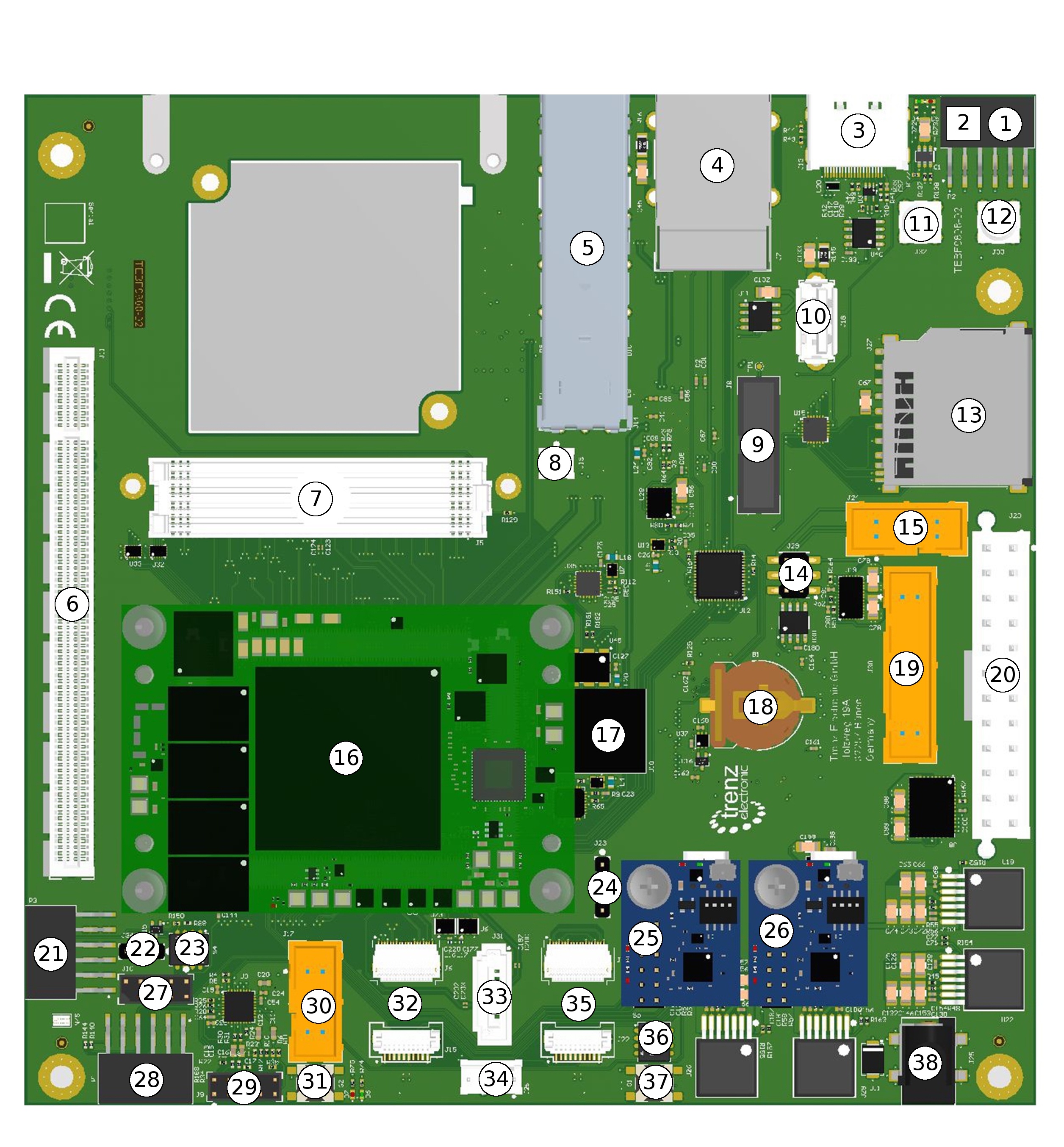
TEBF0808-REV2 Component Locations
| Callout | Feature | Component Designator |
|---|---|---|
| 1 | PMod 2x6 Socket | P2 |
| 2 | MicroSD Connector (Bottom) | J16 |
| 3 | Display Port Socket | J13 |
| 4 | USB3.0 A 2x , RJ45 1x Stacked | J7 |
| 5 | Dual SFP+ | J14 |
| 6 | PCIe x16 Connector (one PCIe lane connected) | J11 |
| 7 | FMC (1.8V max VCCIO) | J5 |
| 8 | FAN-FMC 2 Pol. | J19 |
| 9 | USB3 Connector 19 Pol. | J8 |
| 10 | USB 3.0 A Connector | J18 |
| 11 | SMA (SI5338 CLK1A) | J32 |
| 12 | SMA (B2B-IN2_P) | J33 |
| 13 | SD Card Socket | J27 |
| 14 | CAN PIN-Header 6 Pol. | J29 |
| 15 | CAN Connector 10 Pol. | J24 |
| 16 | 4x Samtec B2B -Connector for TE0808 | J1,J2,J3,J4 |
| 17 | eMMC (MTFC16GJVEC-2M WT) | U2 |
| 18 | Battery holder CR1220 | B1 |
| 19 | JTAG Connector 20 Pol. | J30 |
| 20 | ATX Power supply connector | J20 |
| 21 | PMod 2x6 Socket | P3 |
| 22 | FFA I2C Pin Header | J34 |
| 23 | Jumper 2x4 (Configuration) | S4 |
| 24 | BEEPER PIN Header 4 Pol. | J23 |
| 25 | Pin Header 12 Pol. (XMOD-FPGA Access) | J12 |
| 26 | Pin Header 12 Pol. (XMOD-Carrier CPLD Access) | J28 |
| 27 | Pin Header 9 Pol. (Intel front panel (PWR/RST/LED)) | J10 |
| 28 | PMod 2x6 Socket | P1 |
| 29 | INTEL HDA Header 9 Pol. | J9 |
| 30 | PLL I2C Connector 10 Pol. | J17 |
| 31 | RST Push Button | S2 |
| 32 | Samtec FireFly (4 GT lanes bidirectional) | J6,J15 |
| 33 | SATA Header | J31 |
| 34 | FAN-1 4 Pol. | J26 |
| 35 | Samtec FireFly Connector for reverse loopback | J21,J22 |
| 36 | Jumper 2x4- CPLD | S5 |
| 37 | PWR Push Button | S1 |
| 38 | Power Jack 2.1mm 12V | J25 |
Table: Board Component Description
TE0808 GT Transceivers
| GT Lane | Function | Ref Clock | Comment |
|---|---|---|---|
| PS 0 | PCIe | 100 | |
| PS 1 | USB3 | 100 | |
| PS 2 | SATA | 150 | |
| PS 3 | DP.0 | 27 | |
| B128 0..3 | FireFly | ||
| B228 0..3 | FMC 0..3 | ||
| B229 0..3 | FMC 4..7 | ||
| B230 0.1 | FMC 8..9 | ||
| B230 2 | SFP | 125/156.25 | |
| B230 3 | SFP | 125/156.25 |
GT Lane Assignment
| GT Clock | From | Default | Notes |
|---|---|---|---|
| PS 0 | Oscillator | User | not fitted oscillator |
| PS 1 | Oscillator | 150MHz | SATA |
| PS 2 | Si5345 | 100Mhz | USB/PCIe |
| PS 3 | Si5345 | 27Mhz | DisplayPort |
| B128 0 | Si5345 | ||
| B128 1 | not used | ||
| B228 0 | FMC GTCLK 0 | User | |
| B228 1 | Si5345 | ||
| B229 0 | FMC GTCLK 1 | User | |
| B229 1 | Si5345 | User | |
| B230 0 | Si5345 | User | |
| B230 1 | Si5345 |
GT CLK Assignment
TE0808 MIO Assignment
| MIO | Default | Alternate | Notes |
|---|---|---|---|
| 0..12 | Dual QSPI | - | Bootable |
| 13..23 | SD0: eMMC | - | Bootable |
| 24, 25 | CPLD MUXED | ||
| 26..29 | PJTAG0 | CPLD MUXED | Bootable JTAG |
| 30 | CPLD MUXED | ||
| 31 | PCIe | CPLD MUXED | Same as ZCU102 |
| 32 | CPLD MUXED | ||
| 33 | PMU | CPLD MUXED | Same as ZCU102 |
| 34..37 | DPaux | CPLD MUXED | |
| 38, 39 | I2C0 | - | |
| 40, 41 | CAN1 | CPLD MUXED | |
| 42, 43 | UART0 | CPLD MUXED | |
| 44 | I2C Interrupt | CPLD MUXED | |
| 45..51 | SD1: SD | - | Bootable SD Card |
| 52..63 | USB0 | - | |
| 64..75 | GEM3 | - | |
| 76, 77 | MDIO |
MIO Assignment
TE0808 Si5345 PLL Settings
| Input/Output | Connected to | Frequency | Used as | Notes |
|---|---|---|---|---|
| IN0 | Oscillator | 25MHz | Internal Reference | |
| IN2 | SMA | User | External Reference | |
| OUT0 | PCIe | 100MHz | PCIe REFCLK | |
| OUT1 | B230 CLK0 | 125MHz | FMC GT Clock | |
| OUT2 | B229 CLK1 | User | FMC GT Clock | |
| OUT3 | B228 CLK1 | User | FMC GT Clock | |
| OUT4 | B505 CLK2 | 100MHz | PCIe and USB Clock | |
| OUT5 | B505 CLK3 | 27MHz | DisplayPort GT SERDES Clock | |
| OUT6 | B128 CLK0 | 157.6MHz (2 x 78.8) | DP Video Pixel Clock | Seems to be needed for DP to work |
| OUT7 | B230 CLK1 | 156.25Mhz | SFP Clock | |
| OUT8 | Si5338 IN1 | 25Mhz | Si5338 Reference |
Recommended/Default settings for the Si5345
| Note |
|---|
| By default Si5345 is not programmed after power on, so if FSBL is executed without proper Si5345 init or if psu_init.tcl is invoked and the design does use PS GT, then FSBL or psu_init.tcl would freeze on SERDES init code. Si5345 init does persist over reset sequence so it is possible to use known good boot files to init Si5345 and then FSBL debugging is also possible. |
FMC Slot
FMC Slot is fitted as full FMC HPC.
Note: FMC VADJ maximum voltage is 1.8V (as HP banks do not support more than 1.8V).
| Signals | MPSoC PS/PL | |
|---|---|---|
| FMC LA | HP | Mapped to PL HP Banks |
| FMC HA | HP/HD | HP/HD banks mixed |
| CLK0 | PL Clock | HP Bank |
| CLK1 | PL Clock | HD Bank |
| CLK2 | Clock from Si5345 | use as clock input not supported |
| CLK3 | Clock from Si5345 | use as clock input not supported |
| GT CLK0 | B228 CLK1 | |
| GT CLK1 | B229 CLK1 | |
| I2C | PS I2C | via I2C multplexer |
| GA0, GA1 | 0 | Address set to 00 |
Optional FAN can be mounted below the FMC slot. Ther are no components below the FMC card, so FMC cards with extended component heights can be used.
I2C Buses
| Bus # | Device(s) | Addresses | Notes |
|---|---|---|---|
| 0 | MUX U16 | ||
1 | Si5338 on base | 0x70 | |
| 2 | GPIO Extender | 0x26 | |
| 3 | PCIe SMBus | ||
4 | SFP | ||
| 5 | SFP | ||
| 6 | GPIO, EEPROM | 0x27, 0x50, 0x51, 0x52, 0x54 | |
| 7 | FMC | 0x50 FRU EEPROM | other address depend on FMC Card |
| 8 | USB3 HUB | For REV 2 - DO NOT SCAN will cause I2C bus freeze! | |
| 9 | PMOD | ||
| 10 | ADAU1761 | 0x38 | |
| 11 | FireFly | ||
| 12 | FireFly | ||
| 13 | Si5345 | 0x69 | Access to PLL on TE0808 |
| 14 | CPLD | - | |
| 15 | GPIO | 0x24 | |
| 16 | PMOD |
List of I2C buses and devices (bus numbers as enumerated by Linux).
| Note |
|---|
| Do not scan bus 8, this would cause the I2C bus multiplexer to freeze until power off or hardware reset. |
To init Si5345 use command
si534x /dev/i2c-13 0x69
DIP Switches
There are two 4 bit DIP Switches on the TEBF0808, they must be used to select some options. On TEBF0808-02 default CPLD-Firmware selects boot from SD-Card, Firmware update is needed for Boot-Mode selection.
| 1 | 2 | 3 | 4 | Description |
|---|---|---|---|---|
| ON | ON | ON | ON | Default, boot from SD/eMMC, 1.8V FMC VADJ |
| ON | ON | x | x | Boot from microSD, SD or SPI Flash |
| OFF | ON | x | x | Boot from eMMC |
| ON | OFF | x | x | Boot mode PJTAG0 |
| OFF | OFF | x | x | Boot mode main JTAG |
| x | x | x | ON | FMC VADJ = 1.8V |
| x | x | x | OFF | FMC VADJ = 1.2V |
DIP Switch S5 located close to PWR push-button. This DIP Switch is connected to the two baseboard control CPLD's.
| 1 | 2 | 3 | 4 | Description |
|---|---|---|---|---|
| OFF | OFF | OFF | ON | Default |
| ON | x | x | x | PUDC = 0 |
| OFF | x | x | x | PUDC = High |
DIP Switch S4 located close to PCIe slot.
LEDs
| LED | Position | Description |
|---|---|---|
| D4 | Green LED near DisplayPort Connector | |
| D5 | Red LED near DisplayPort Connector | |
| D6 | Green LED near Reset Button | |
| D7 | Red LED near Reset Button |
Power
ATX Power is supported but special 12V ATX power supply must be used.
System controller RGPIO
Master CPLD Read
Bit | Description |
|---|---|
| 31 | '1' - Constant value |
| 30 | '0' - Constant value |
| 29 | '1' - Constant value |
| 28 | '0' - Constant value |
| 27 | |
| 26 | |
| 25 | |
| 24 | |
| 23 | |
| 22 | |
| 21 | SCL |
| 20 | SDA |
| 19 | DP PHD |
| 18 | JTAG TMS |
| 17 | JTAG TDI |
| 16 | JTAG TCK |
| 15 | JTAG SRST |
| 14 | JTAG TRST |
| 13 | FMC CLKDIR |
| 12 | FMC TDO |
| 11 | PHY LED2 |
| 10 | PHY LED1 |
| 9 | PHY LED0 |
| 8 | CAN Fault |
| 7 | MIO29 |
| 6 | MIO28 |
| 5 | MIO27 |
| 4 | MIO26 |
| 3 | XMOD Button |
| 2 | SD WP |
| 1 | SW4 |
| 0 | SW3 |
Master CPLD Write
Bit | Description |
|---|---|
| 31 | '1' - Constant value |
| 30 | '0' - Constant value |
| 29 | '1' - Constant value |
| 28 | '0' - Constant value |
| 27 | |
| 26 | |
| 25 | |
| 24 | |
| 23 | |
| 22 | |
| 21 | |
| 20 | |
| 19 | |
| 18 | |
| 17 | |
| 16 | |
| 15 | |
| 14 | JLED2B |
| 13 | JLED2A |
| 12 | JLED1 |
| 11 | SFP_LED3 |
| 10 | SFP_LED2 |
| 9 | SFP_LED1 |
| 8 | SFP_LED0 |
| 7 | LED1 |
| 6 | LED0 |
| 5 | USB HUB MODE1 ('1' for ROM Mode) |
| 4 | USB HUB MODE0 ('1' for ROM Mode) |
| 3 | Ethernet PHY Reset (Active High) |
| 2 | I2C Reset (Active High) |
| 1 | USB HUB Reset (Active High) |
| 0 | USB PHY Reset (Active High) |
Slave CPLD Read
Bit | Description |
|---|---|
| 31 | '1' - Constant value |
| 30 | '0' - Constant value |
| 29 | '1' - Constant value |
| 28 | '0' - Constant value |
| 27 | |
| 26 | |
| 25 | |
| 24 | |
| 23 | |
| 22 | |
| 21 | |
| 20 | |
| 19 | |
| 18 | |
| 17 | |
| 16 | |
| 15 | |
| 14 | |
| 13 | |
| 12 | |
| 11 | |
| 10 | |
| 9 | PLL LOL |
| 8 | XMOD Button |
| 7 | Power OK |
| 6 | Fan Senese |
| 5 | SD Detect |
| 4 | Micro SD Detect |
| 3 | Power Button |
| 2 | Reset Button |
| 1 | SW2 |
| 0 | SW1 |
Slave CPLD Write
Bit | Description |
|---|---|
| 31 | '1' - Constant value |
| 30 | '0' - Constant value |
| 29 | '1' - Constant value |
| 28 | '0' - Constant value |
| 27 | |
| 26 | |
| 25 | |
| 24 | |
| 23 | |
| 22 | |
| 21 | |
| 20 | |
| 19 | |
| 18 | |
| 17 | |
| 16 | |
| 15 | |
| 14 | |
| 13 | |
| 12 | |
| 11 | FAN_EN |
| 10 | HDLED_P |
| 9 | HDLED_N |
| 8 | LED_P |
| 7 | LED_N |
| 6 | LED3 |
| 5 | LED2 |
| 4 | FPGA PROG (Active High) |
| 3 | PCIe Reset (Active High) |
| 2 | MRESET Reset (Active High) |
| 1 | SRST Reset (Active High) |
| 0 | PLL Reset (Active High) |
PCB Revisions
Revision 02
Known Issues:
- signal SFP1 LOS is not connected (fixed in REV 03)
Revision 03
Overview
Content Tools