Page History
...
All MIO banks are powered from on-module DC-DC power rail. All PL I/O Banks banks have separate VCCO input pins in the B2B connectors, valid VCCO should be supplied from the baseboardcarrier board.
For detailed information about the B2B pin-out, please refer to the Pin-out table.
...
| Signal | B2B Connector Pin | Function |
|---|---|---|
| DONE | J2-116 | PL configuration completed |
| PROG_B | J2-100 | PL configuration reset signal |
| INIT_B | J2-98 | PS is initialized after a power-on reset |
| SRST_B | J2-96 | System reset |
| MODE0 ... MODE3 | J2-109/J2-107/J2-105/J2-103 | 4-bit boot mode pins For further information about the boot-modes refer to the Xilinx Zynq UltrascaleUltraScale+ MPSoC TRM |
| ERR_STATUS / ERR_OUT | J2-86 / J2-88 | ERR_OUT signal is asserted for accidental loss of ERR_STATUS indicates a secure lockdown state |
| PUDC_B | J2-127 | Pull-up during configuration (pulled-up to 'PL_1V8') |
...
The boot source of the Zynq UltraScale+ MPSoC can be selected via 4 dedicated pins, which generate a 4-bit code to select the boot mode. The pins are accessible on B2B connector J2:
...
Following boot modes are possible on the TE0803 UltraScale+ MPSoC module by generating the corresponding 4-bit code by the with pins 'PS_MODE0' ... 'PS_MODE3' (little-endian alignment):
...
For Functional details see ug1085 - Zynq UltraScale+ TRM (Boot Modes Section).
...
| Name | IC | Designator | PS7 | MIO | Notes |
|---|---|---|---|---|---|
| SPI Flash | N25Q256A11E1240E | U7 | QSPI0 | MIO0 ... MIO5 | dual Dual parallel booting possible, 32 MByte memory per Flash IC at standard configuration |
| SPI Flash | N25Q256A11E1240E | U17 | QSPI0 | MIO7 ... MIO12 | as As above |
Table 10: Peripherals connected to the PS MIO - pins
DDR4 SDRAM
The TE0803-01 SoM is equipped with with four DDR4-2400 SDRAM modules with up to 8 GByte memory density. The SDRAM modules are connected to the Zynq MPSoC's PS DDR - controller (bank 504) with a 64-bit databus data bus width.
Refer to the Xilinx Zynq UltrascaleUltraScale+ data sheet DS925 to get information, if the specific package of the Zynq UltrascaleUltraScale+ MPSoC equipped on module supports the maximum data transmission rate of 2400 MByte/s.
...
| Note |
|---|
Si5338A OTP ROM is not programmed by default at delivery, so it is customers responsibility to either configure Si5338A during FSBL or then use SiLabs Silicon Labs programmer and burn the OTP ROM with customer fixed clock setup. |
Si5338A OTP can only be programmed two times, as different user configurations may required different setup TE0803 is normally shipped with blank OTP.
For Refer to Si5338A datasheet for more informationSi5338A at SiLabs.
Clocking
The TE0803-01 SoM is equipped with two on-board oscillators to provide the Zynq MPSoC's PS configuration bank 503 with reference clock - signals.
| Clock | Frequency | Bank 503 Pin | Connected to |
|---|---|---|---|
| PS_CLK | 33.333333 MHz | R16 | MEMS Oscillatoroscillator, U32 |
| PS_PAD (RTC) | 32.768 kHz | N17/N18 | Quartz crystal, Y2 |
...
| LED | Color | Connected to | Description and Notes |
|---|---|---|---|
| D1 | redRed | DONE signal (PS Configuration Bank 503) | This LED goes ON when power has been applied to the module and stays ON until MPSoC's programmable logic is configured properly. |
...
Table 15: Maximum current of power supplies. *to be determined To Be Determined soon with reference design setup.
...
The TE0803 module equipped with the Xilinx Zynq UltrascaleUltraScale+ MPSoC delivers a heterogeneous multi-processing system with integrated programmable logic and independently operable elements and is designed to meet embedded system power management requirement by advanced power management features. This features allow to offset the power and heat constraints against overall performance and operational efficiency.
This features allowing highly flexible power management are achieved by establishing Power Domains for power isolation. The Zynq UltraScale+ MPSoC has multiple power domains, whereby each power domain requires its own particular extern DCDC external DC-DC converters.
The Processing System contains three Power Domains:
...
| Enable-Signal | B2B Connector Pin | Max. Voltage | Note | Power-Good-Signal | B2B Connector Pin | Pull-up Resistor | Note | |
|---|---|---|---|---|---|---|---|---|
| EN_LPD | J2-108 | 6V | TPS82085SIL data sheet | LP_GOOD | J2-106 | 4K7, pulled up to LP_DCDC | - | |
| EN_FPD | J2-102 | DCDCIN | NC7S08P5X data sheet | PG_FPD | J2-110 | 4K7, pulled up to DCDCIN | - | |
| EN_PL | J2-101 | max PL_DCIN | left Left floating for logic high (drive to GND for logic low) | PG_PL | J2-104 | external External pull-up needed (max. voltage 'GT_DCDC'), maxMax. sink current 1 mA | TPS82085SIL / | |
| EN_DDR | J2-112 | DCDCIN | NC7S08P5X data sheet | PG_DDR | J2-114 | 4K7, pulled up to DCDCIN | - | |
| EN_PSGT | J2-84 | DCDCIN | NC7S08P5X data sheet | PG_PSGT | J2-82 | external External pull-up needed (max. 5.5V), maxMax. sink current 1 mA | TPS74801 data sheetdatasheet | |
| EN_GT_R | J2-95 | GT_DCDC | NC7S08P5X data sheet | PG_GT_R | J2-91 | external External pull-up needed (max. 5.5V), maxMax. sink current 1 mA | TPS74401 data sheetdatasheet | |
| - | - | - | - | PG_VCU_1V0 | J2-97 | external External pull-up needed (max. 5.5V), | TPS82085SIL data sheetdatasheet |
Table 16: Recommended operation conditions of DC-DC converter control signals
...
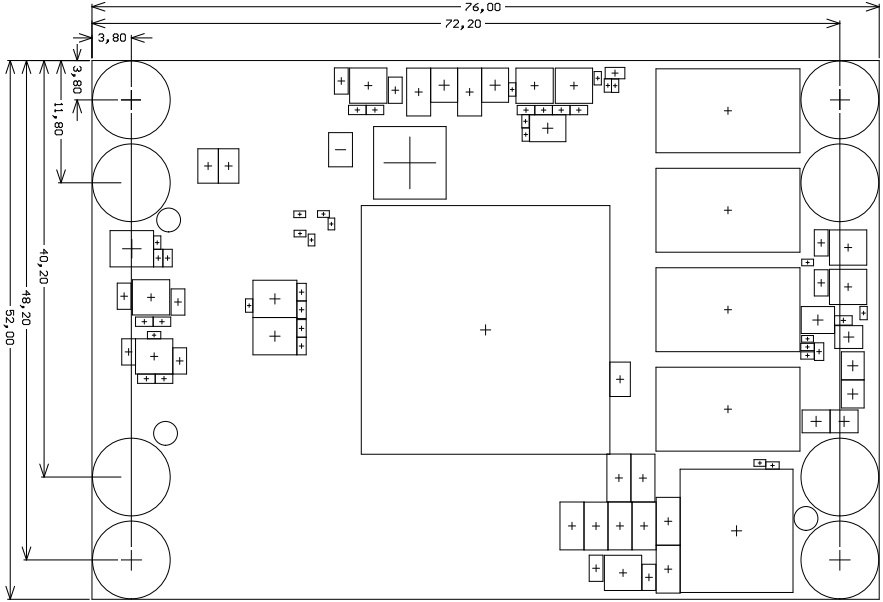
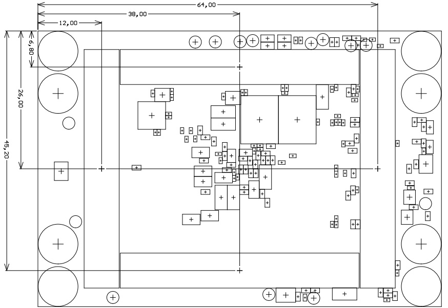
All dimensions are given in millimeters.
Revision History
...
| Date | Revision | Notes | Link to PCN | Documentation Link |
|---|---|---|---|---|
| 2016-12-23 | 01 | First production release | - | TE0803-01 |
...
Overview
Content Tools