Page History
| Scroll Ignore |
|---|
Download PDF version of this document. |
| Scroll pdf ignore | |
|---|---|
Table of Contents
|
Overview
| Scroll Only (inline) |
|---|
Refer to https://wiki.trenz-electronic.de/display/PD/TE0841+TRM for online version of this manual and additional technical documentation of the product. |
The Trenz Electronic TE0841-01 is an industrial-grade 4 x 5 cm SoM integrating Xilinx Kintex UltraScale KU035 FPGA, 2 banks of 512 MByte DDR4 SDRAM, 32 MByte QSPI Flash for configuration and operation, and powerful switch-mode power supplies for all on-board voltages. Numerous configurable I/Os are provided via rugged high-speed strips. All this on a tiny footprint, smaller than a credit card size at very competitive price. All Trenz Electronic 4 x 5 cm SoMs are mechanically compatible.
Key Features
- Xilinx Kintex UltraScale FPGA (XCKU035 or XCKU040)
- 2 banks of 512 MByte, 16 bit wide DDR4 SDRAM
- 256 Mbit (32 MByte) QSPI Flash
- 3 x Samtec Razor Beam LSHM B2B, 260 terminals total
- User I/O: 60 x HR, 84 x HP
- Serial transceiver: 8 x GTH lanes (TX/RX)
- GT clock inputs: 2 - Clocking
- Si5338 - 4 output PLLs, GT and PL clocks
- 200 MHz LVDS oscillator - All power supplies on-board, single power source operation
- Evenly spread supply pins for optimized signal integrity
- Size: 40 x 50 mm
- 3 mm mounting holes for skyline heat spreader
- Rugged for industrial applications
Additional assembly options for cost or performance optimization plus high volume prices are available on request.
Block Diagram
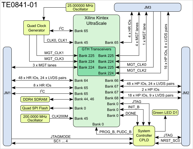
Main Components
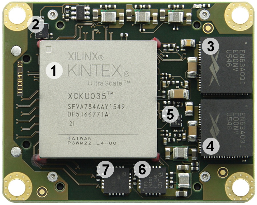
- Xilinx Kintex UltraScale FPGA, U1
- Ultra performance oscillator @25.000000 MHz, U3
- 12A PowerSoC DC-DC converter (0.95V), U14
- 12A PowerSoC DC-DC converter (0.95V), U7
- Low-jitter precision LVDS oscillator @200.0000 MHz, U11
- Low-dropout (LDO) linear regulator (MGTAVTT 1.20V), U8
- Low-dropout (LDO) linear regulator (MGTAVCC 1.02V), U12
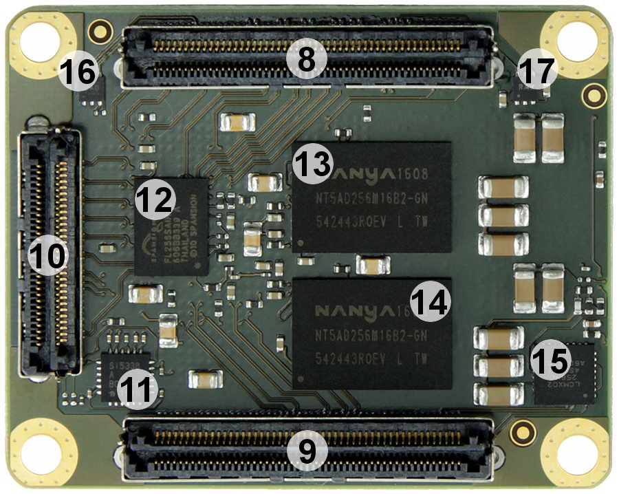
- Samtec Razor Beam™ LSHM-150 B2B connector, JM1
- Samtec Razor Beam™ LSHM-150 B2B connector, JM2
- Samtec Razor Beam™ LSHM-130 B2B connector, JM3
- Programmable quad clock generator, U2
- 32 MByte QSPI Flash, U6
- 4 Gbit DDR4 SDRAM, U4
- 4 Gbit DDR4 SDRAM, U5
- System Controller CPLD, U18
- Low-dropout (LDO) linear regulator (MGTAUX), U9
- Ultra-low power low-dropout (LDO) regulator (VBATT), U19
Initial Delivery State
Storage device name | Content | Notes |
|---|---|---|
OTP Flash area | Empty |
Signals, Interfaces and Pins
Board to Board (B2B) I/Os
I/O signals connected from the SoCs I/O banks and B2B connectors:
| FPGA Bank | Type | B2B Connector | I/O Signal Count | Voltage | Notes |
|---|---|---|---|---|---|
| 64 | HR | JM1 | 48 IOs, 24 LVDS pairs | B64_VCCO | Supplied by the carrier board. |
| 65 | HR | JM1 | 8 IOs | 3.3V | |
| 224 | MGT | JM1 | 3 lanes | ||
| 65 | HR | JM3 | 4 IOs, 2 LVDS pairs | 3.3V | |
| 66 | HP | JM3 | 16 IOs, 8 LVDS pairs | B66_VCCO | Supplied by the carrier board |
| 224 | MGT | JM3 | 1 lane | ||
| 225 | MGT | JM3 | 4 lanes | ||
| 67 | HP | JM2 | 48 IOs, 24 LVDS pairs | B67_VCCO | Supplied by the carrier board |
| 67 | HP | JM2 | 2 IOs | B67_VCCO | Supplied by the carrier board |
| 68 | HP | JM2 | 18 IOs, 9 LVDS pairs | B68_VCCO | Supplied by the carrier board |
For detailed information about the pin out, please refer to the Pin-out Tables.
JTAG Interface
JTAG access to the Xilinx Kintex UltraScale FPGA is available through B2B connector JM2.
JTAG Signal | B2B Connector Pin |
|---|---|
| TMS | JM2-93 |
| TDI | JM2-95 |
| TDO | JM2-97 |
| TCK | JM2-99 |
| Note |
|---|
| JTAGMODE pin 89 in B2B connector JM1 should be kept low or grounded for normal operation. |
System Controller CPLD I/O Pins
Special purpose pins are connected to the System Controller CPLD and have following default configuration:
| Pin Name | Mode | Function | Default Configuration |
|---|---|---|---|
| JTAGMODE | Input | JTAG select | Low for normal operation. |
| NRST_SC0 | Input | Reset | |
| SC1 | - | - | Not used by default. |
| SC2 | - | - | Not used by default. |
| SC3 | - | - | Not used by default. |
| SC4 | - | - | Not used by default. |
On-board LEDs
| LED | Color | Connected to | Description and Notes |
|---|---|---|---|
| D1 | Green | System Controller CPLD, bank 3 | Exact function is defined by SC CPLD firmware. |
I2C Interface
There are two PL bank 65 IO pins (PLL_SCL and PLL_SDA) reserved as I2C bus connected to the Si5338 PLL quad clock generator. Default Si5338 PLL chip I2C bus slave address is 0x70.
Additionally, two PL bank 65 IO pins (B65_SCL and B65_SDA) connected to the B2B connector JM1 can be used for external I2C connectivity, otherwise these pins are ordinary IOs.
On-board Peripherals
Processing System (PS) Peripherals
| Name | IC | ID | PS7 | MIO | Notes |
|---|---|---|---|---|---|
| QSPI Flash | N25Q256A | U6 | |||
| PLL quad clock generator | SI5338A | U2 |
Clocking
| Clock Signal | Frequency | Source | FPGA | Notes |
|---|---|---|---|---|
| - | 25.000000 MHz | SiT8208 (U3), CLK | - | Reference clock input for Si5338 PLL quad clock generator. |
| CLK200M | 200.0000 MHz | DSC1123 (U11), OUT | R25/R26, bank 45 | |
| CLK0 | User programmable | Si5338 (U2), CLK3 | T24/T25, bank 45 | |
| CLK1 | User programmable | Si5338 (U2), CLK0 | R23/P23, bank 45 | |
| MGT_CLK0 | Supplied by the carrier board | JM3-31, JM3-33 | Y5/Y6, bank 225 | Bank 225 MGTs clock source from baseboard. |
| MGT_CLK1 | User programmable | Si5338 (U2), CLK1 | V5/V6, bank 225 | Bank 225 MGTs clock source from on-board PLL quad clock generator. |
| MGT_CLK2 | Supplied by the carrier board | JM3-32, JM3-34 | AD6/AD5, bank 224 | Bank 224 MGTs clock source from baseboard. |
| MGT_CLK3 | User programmable | Si5338 (U2), CLK2 | AB6/AB5, bank 224 | Bank 224 MGTs clock source from on-board PLL quad clock generator. |
Power and Power-On Sequence
Power Supply
Single 3.3V power supply with minimum current capability of 4A for system startup is recommended.
Power Consumption
| Power Input Pin | Typical Current |
|---|---|
| VIN | TBD* |
| 3.3VIN | TBD* |
* TBD - To be determined.
Power-On Sequence
For highest efficiency of the on-board DC-DC regulators, it is recommended to use same 3.3V power source for both VIN and 3.3VIN power rails. Although VIN and 3.3VIN can be powered up in any order, it is recommended to power them up simultaneously.
It is important that all baseboard I/Os are 3-stated at power-on until System Controller CPLD sets PGOOD signal high (B2B connector JM1, pin 30), or 3.3V is present on B2B connector JM2 pins 10 and 12, meaning that all on-module voltages have become stable and module is properly powered up.
See also Xilinx datasheet DS892 for additional information. User should also check related baseboard documentation when choosing baseboard design for TE0720 module.
Power Rails
Voltages on B2B Connectors | B2B JM1 Pins | B2B JM2 Pins | Input/Output | Notes |
|---|---|---|---|---|
| VIN | 1, 3, 5 | 2, 4, 6, 8 | Input | Supply voltage. |
| 3.3VIN | 13, 15 | - | Input | Supply voltage. |
| B64_VCO | 9, 11 | - | Input | HR (High Range) bank voltage. |
| B66_VCO | - | 1, 3 | Input | HP (High Performance) bank voltage. |
| B67_VCO | - | 7, 9 | Input | HP (High Performance) bank voltage. |
| B68_VCO | - | 5 | Input | HP (High Performance) bank voltage. |
VBAT_IN | 79 | - | Input | RTC battery supply voltage. |
| 3.3V | - | 10, 12, 91 | Output | Module on-board 3.3V voltage level. |
Board to Board Connectors
| Include Page | ||||
|---|---|---|---|---|
|
Variants Currently In Production
| Module Variant | FPGA Chip | Temperature Range |
|---|---|---|
| TE0841-01-035-1C | XCKU035-1SFVA784C | Commercial |
TE0841-01-035-1I | XCKU035-1SFVA784I | Industrial |
TE0841-01-035-2I | XCKU035-2SFVA784I | Industrial |
| TE0841-01-040-1C | XCKU040-1SFVA784C | Commercial |
| TE0841-01-040-1I | XCKU040-1SFVA784I | Industrial |
Technical Specifications
Absolute Maximum Ratings
Parameter | Min | Max | Units | Reference Document |
|---|---|---|---|---|
VIN supply voltage | V | - | ||
| Supply voltage for HR I/O banks (VCCO) | –0.500 | 3.400 | V | See Xilinx datasheet DS892. |
Supply voltage for HP I/O banks (VCCO) | –0.500 | 2.000 | V | See Xilinx datasheet DS892. |
| I/O input voltage for HR I/O banks | –0.400 | VCCO + 0.550 | V | See Xilinx datasheet DS892. |
I/O input voltage for HP I/O banks | –0.550 | VCCO + 0.550 | V | See Xilinx datasheet DS892. |
| GTH and GTY transceiver reference clocks absolute input voltage (MGT_CLK0, MGT_CLK2) | -0.500 | 1.320 | V | See Xilinx datasheet DS892. |
GTH and GTY transceiver receiver (RXP/RXN) and transmitter (TXP/TXN) absolute input voltage | -0.500 | 1.260 | V | See Xilinx datasheet DS892. |
Storage temperature | -40 | +85 | °C | - |
Recommended Operating Conditions
| Parameter | Min | Max | Units | Reference Document |
|---|---|---|---|---|
| VIN supply voltage | ||||
| Supply voltage for HR I/O banks (VCCO) | 1.140 | 3.400 | V | See Xilinx datasheet DS892. |
Supply voltage for HP I/O banks (VCCO) | 0.950 | 1.890 | V | See Xilinx datasheet DS892. |
I/O input voltage | –0.200 | VCCO + 0.20 | V | See Xilinx datasheet DS892. |
| Note |
|---|
| Assembly variants for higher storage temperature range are available on request. |
Operating Temperature Ranges
Commercial grade: 0°C to +70°C.
Industrial grade: -40°C to +85°C.
Operating temperature range depends also on customer design and cooling solution. Please contact us for options.
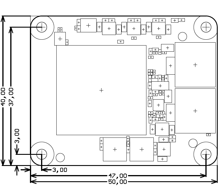
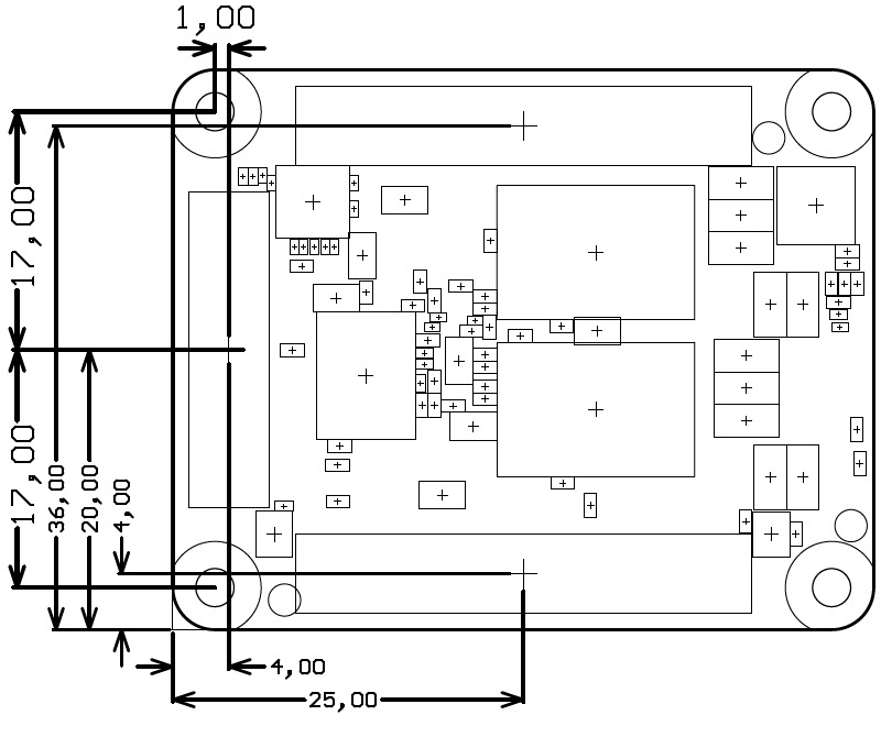
Physical Dimensions
Module size: 50 mm × 40 mm. Please download the assembly diagram for exact numbers.
Mating height with standard connectors: 8 mm.
PCB thickness: 1.6 mm.
Highest part on PCB: approximately 3 mm. Please download the step model for exact numbers.
All dimensions are given in millimeters.
Weight
47 g - Plain module.
9 g - Set of bolts and nuts.
Revision History
Hardware Revision History
| Date | Revision | Notes | PCN | Documentation Link |
|---|---|---|---|---|
| 2015-12-09 | 01 | First production revision | - | TE0841-01 |
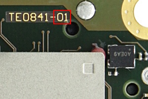
Hardware revision number is printed on the PCB board together with the module model number separated by the dash.
Document Change History
Date | Revision | Contributors | Description |
|---|---|---|---|
| 2017-06-14 | Jan Kumann | Initial document. |
Disclaimer
| Include Page | ||||
|---|---|---|---|---|
|
Overview
Content Tools