Page History
...
Adjustable PL Bank VCCO Voltage FMC_VADJ
Power Distribution Dependencies
The power rails 'DCDCIN', 'LP_DCDC', 'PL_DCIN', 'PS_BATT' have to be powered up on the assigned pins of the B2B connectors as listed on the section "Power Rails". Except 'PS_BATT' (see section "Recommended Operation Conditions"), all power-rails can be powered up, with 3.3V power sources, also shared, if Power Domain control is not required.
There are following dependencies how the initial voltages of the power rails on the B2B connectors are distributed to the on-board DCDC converters, which power up further DCDC converters and the particular on-board voltages:
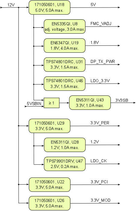
Figure 11: Power Distribution Diagram
| Note |
|---|
Current rating of Samtec Razor Beam™ LSHM B2B connectors is 2.0A per pin (2 adjacent pins powered). |
Power-On Sequence Diagram
The TE0808 SoM meets the recommended criteria to power up the Xilinx Zynq Ultrascale+ MPSoC properly by keeping a specific sequence of enabling the on-board DCDC converters dedicated to the particular Power Domains and powering up the on-board voltages.
The on-board voltages of the TE0808 SoM will be powered-up in order of a determined sequence by activating the above-mentioned power rails and the Enable-Signals of the DCDC converters. The on-board voltages will be powered up at three steps.
- Low-Power Domain (LPD) and on-board Si5345A programmable clock generator supply voltage
- Programmable Logic (PL) and Full-Power Domain (FPD)
- GTH, PS GTR transceiver and DDR memory
Hence, those three power instances will be powered up consecutively and the Power-Good-Signals of the previous instance has to be asserted.
Following diagram clarifies the sequence of enabling the three power instances utilizing the DCDC converter control signals ('Enable', 'Power-Good'), which will power-up in descending order as listed in the blocks of the diagram.
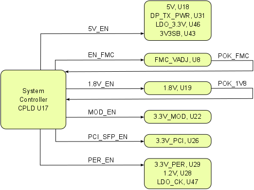
Figure 12: Power-On Sequence Utilizing DCDC Converter Control Signals
| Warning |
|---|
| To avoid any damages to the MPSoC module, check for stabilized on-board voltages in steady state before powering up the MPSoC's I/O bank voltages VCCOx. All I/O's should be tri-stated during power-on sequence. |
Core voltages and main supply voltages have to reach stable state and their "Power Good"-signals have to be asserted before other voltages like bank's I/O voltages (VCCOx) can be powered up.
It is important that all PS and PL I/Os are tri-stated at power-on until the "Power Good"-signals are high, meaning that all on-module voltages have become stable and module is properly powered up.
See Xilinx datasheet DS925 for additional information. User should also check related base board documentation when intending base board design for TE0808 SoM.
Power Rails
...
Voltages on B2B
Connectors
...
Input/
Output
...
-
...
J2-154, J2-156, J2-158, J2-160,
J2-153, J2-155, J2-157, J2-159
...
Internal voltage level
1.8V nominal output
...
Internal voltage level
1.8V nominal output
...
Internal voltage level
1.2V nominal output
The carrier board VCCO voltage 'FMC_VADJ' supplying the PL IO-banks of the SoM (bank 64, 65, 66, 48) is provided by DC-DC converter U8 and selectable by the pins 'FMC_VID0' ... 'FMC_VID2' of the System Controller CPLD U17.
| FMC_VID2 | FMC_VID1 | FMC_VID0 | FMC_VADJ Value |
|---|---|---|---|
| 0 | 1 | 0 | 1.8V |
| 0 | 1 | 1 | 1.5V |
| 1 | 0 | 0 | 1.25V |
| 1 | 0 | 1 | 1.2V |
Table 3: Bit patterns for fixed values of the FMC_VADJ voltage
Note: These pins of the DC-DC converter U8 are initialiy hardwired to fix the voltage to 1.8V (see schematic).
Power Distribution Dependencies
All on-board voltages of the TEBF0808 are generated out of the extern applied 12V power supply.
There are following dependencies how the initial 12V power supply is distributed to the on-board DC-DC converters, which power up further DCDC converters and the particular on-board voltages:
Figure 11: Power Distribution Diagram
| Note |
|---|
Current rating of Samtec Razor Beam™ LSHM B2B connectors is 2.0A per pin (2 adjacent pins powered). |
Power-On Sequence Diagram
The power-on sequence of the on-board DC-DC converters depens on the current firmware of the System Controller CPLD U17.
Following diagram visualizes the connection of the DC-DC converter control signals ('Enable', 'Power-Good') with System Controller CPLD U17, which enables the particular on-board voltages.
Figure 12: Power-On Sequence Utilizing DCDC Converter Control Signals
| Warning |
|---|
| To avoid any damages to the MPSoC module, check for stabilized on-board voltages in steady state before powering up the MPSoC's I/O bank voltages VCCOx. All I/O's should be tri-stated during power-on sequence. |
Core voltages and main supply voltages of the Zynq Ultrascale+ MPSoC have to reach stable state and the "Power Good"-signals of the SoM have to be asserted before other voltages like bank's I/O voltages (VCCOx) can be powered up.
It is important that all PS and PL I/Os are tri-stated at power-on until the "Power Good"-signals are logically high, meaning that all on-module voltages have become stable and module is properly powered up.
Power Rails
Voltages on B2B | B2B J1 Pin | B2B J2 Pin | B2B J3 Pin | B2B J4 Pin | Input/ | Note |
|---|---|---|---|---|---|---|
| PL_DCIN | J1-151, J1-153, J1-157, J1-159 | - | - | - | Input | - |
| DCDCIN | - | J2-154, J2-156, J2-158, J2-160, | - | - | Input | - |
| LP_DCDC | - | J2-138, J2-140, J2-142, J2-144 | - | - | Input | - |
| PS_BATT | - | J2-125 | - | - | Input | - |
| GT_DCDC | - | - | J3-157, J3-158, J3-159, J3-160 | - | Input | - |
| PLL_3V3 | - | - | J3-152 | - | Input | U5 (programmable PLL) 3.3V nominal input |
| SI_PLL_1V8 | - | - | J3-151 | - | Output | Internal voltage level 1.8V nominal output |
| PS_1V8 | - | J2-99 | J3-148 | - | Output | Internal voltage level |
| PL_1V8 | J1-91, J1-121 | - | - | - | Output | Internal voltage level |
| DDR_1V2 | - | J2-135 | - | - | Output | Internal voltage level |
Table 17: Power rails of the MPSoC module on accessible connectors
Bank Voltages
| Bank | Type | Schematic Name / B2B connector Pins | Voltage | Reference Input Voltage | Voltage Range |
|---|---|---|---|---|---|
| 47 | HD | VCCO47, pins J3-43, J3-44 | user | - | max. 3.3V |
| 48 | HD | VCCO48, pins J3-15, J3-16 | user | - | max. 3.3V |
| 64 | HP | VCCO64, J4-58, J4-106 | user | VREF_64, pin J4-88 | max. 1.8V |
| 65 | HP | VCCO65, J4-69, J4-105 | user | VREF_65, pin J4-15 | max. 1.8V |
| 66 | HP | VCCO66, J1-90, J1-120 | user | VREF_66, pin J1-108 | max. 1.8V |
| 500 | MIO | PS_1V8 | 1.8V | - | - |
| 501 | MIO | PS_1V8 | 1.8V | - | - |
| 502 | MIO | PS_1V8 | 1.8V | - | - |
| 503 | CONFIG | PS_1V8 | 1.8V | - | - |
Table 18: Range of MPSoC module's bank voltagesTable 17: Power rails of the MPSoC module on accessible connectors
B2B connectors
| Include Page | ||||
|---|---|---|---|---|
|
...
Parameter | Min | Max | Unit | Notes / Reference Document |
|---|---|---|---|---|
| PL_DCIN | -0.3 | 7 | V | TPS82085SIL / EN63A0QI data sheet |
| DCDCIN | -0.3 | 7 | V | TPS82085SIL / TPS51206 data sheet |
| LP_DCDC | -0.3 | 4 | V | TPS3106K33DBVR data sheet |
| GT_DCDC | -0.3 | 7 | V | TPS82085SIL data sheet |
Storage temperature (ambient) | -40 | 100 | °C | ROHM Semiconductor SML-P11 Series data sheet |
| Note |
|---|
| Assembly variants for higher storage temperature range are available on request. |
...
Overview
Content Tools