Page History
...
| Pin Name | Mode | Function | Default Configuration |
|---|---|---|---|
| JTAGMODE | Input | JTAG select | Low for normal operation. |
| NRST_SC0 | Input | Reset | |
| SC1 | - | - | Not used by default. |
| SC2 | - | - | Not used by default. |
| SC3 | - | - | Not used by default. |
| SC4 | - | - | Not used by default. |
Table 6: System Controller CPLD I/O pins.
Quad SPI Interface
Quad SPI Flash (U6) interface is connected to the FPGA configuration bank 0.
| Signal Name | U6 Pin | FPGA Pin |
|---|---|---|
| SPI_CS | C2 | RDWR_FCS_B_0, AH7 |
| SPI_D0 | D3 | D00_MOSI_0, AA7 |
| SPI_D1 | D2 | D01_DIN_0, Y7 |
| SPI_D2 | C4 | D02_0, U7 |
| SPI_D3 | D4 | D03_0, V7 |
| SPI_CLK | B2 | CCLK_0, V11 |
Table 7: Quad SPI interface signals and connections.
I2C Interface
There are two PL bank 65 IO I/O pins (PLL_SCL and PLL_SDA) reserved as I2C bus connected to the Si5338 PLL quad clock generator. Default Si5338 PLL chip I2C bus slave address is 0x70.
Additionally, two PL bank 65 IO I/O pins (B65_SCL and B65_SDA) connected to the B2B connector JM1 can be used for external I2C connectivity, otherwise these pins are ordinary IOsI/Os.
On-board Peripherals
System Controller CPLD
...
| Si5338A Pin | Signal Name / Description | Connected To | Direction | Note |
|---|---|---|---|---|
IN1 | - | Not connected. | Input | Not used. |
| IN2 | - | GND | Input | Not used. |
IN3 | Reference input clock. | U3, pin 3 | Input | 25.000000 MHz oscillator, Si8208AI. |
IN4 | - | GND | Input | I2C slave device address LSB. |
IN5 | - | Not connected. | Input | Not used. |
| IN6 | - | GND | Input | Not used. |
CLK0A | CLK1_P | U1, R23 | Output | FPGA bank 45. |
| CLK0B | CLK1_N | U1, P23 | Output | FPGA bank 45. |
| CLK1A | MGT_CLK1_N | U1, V5 | Output | FPGA MGT bank 225 reference clock. |
| CLK1B | MGT_CLK1_P | U1, V6 | Output | FPGA MGT bank 225 reference clock. |
| CLK2A | MGT_CLK3_N | U1, AB5 | Output | FPGA MGT bank 224 reference clock. |
| CLK2B | MGT_CLK3_P | U1, AB6 | Output | FPGA MGT bank 224 reference clock. |
| CLK3A | CLK0_P | U1, pin T24 | Output | FPGA bank 45. |
| CLK3B | CLK0_N | U1, pin T25 | Output | FPGA bank 45. |
Table 8: Programmable quad PLL clock generator inputs and outputs.
Oscillators
The FPGA module has following reference clocking signals provided by external baseboard sources and on-board oscillators:
| Clock Source | Frequency | Signal Name | Clock Destination | ||||
|---|---|---|---|---|---|---|---|
| U3, SiT8208AI | |||||||
| Clock Signal | Frequency | Source | FPGA | Notes | |||
| - | 25.000000 MHz | SiT8208 (U3), CLK | - | Reference clock input for Si5338 PLL quad clock generator. | CLK | U2, pin 3 (IN3) | |
| U11, DSC1123DL5CLK200M | 200.0000 MHz | DSC1123 (U11), OUT | R25/R26, bank 45 | ||||
| CLK0 | User programmable | Si5338 (U2), CLK3 | T24/T25, bank 45 | ||||
| CLK1 | User programmable | Si5338 (U2), CLK0 | R23/P23, bank 45 | ||||
| MGT_CLK0 | Supplied by the carrier board | JM3-31, JM3-33 | Y5/Y6, bank 225 | Bank 225 MGTs clock source from baseboard. | |||
| MGT_CLK1 | User programmable | Si5338 (U2), CLK1 | V5/V6, bank 225 | Bank 225 MGTs clock source from on-board PLL quad clock generator. | |||
| MGT_CLK2 | Supplied by the carrier board | JM3-32, JM3-34 | AD6/AD5, bank 224 | Bank 224 MGTs clock source from baseboard. | |||
| MGT_CLK3 | User programmable | Si5338 (U2), CLK2 | AB6/AB5, bank 224 | Bank 224 MGTs clock source from on-board PLL quad clock generator. |
Oscillators
The FPGA module has following reference clocking signals provided by external baseboard sources and on-board oscillators:
...
| CLK200M_P | U1, pin R25 | ||
| U11, DSC1123DL5 | 200.0000 MHz | CLK200M_N | U1, pin R26 |
| B2B, JM3-31 | User | MGT_CLK0_N | U1, pin Y5 |
| B2B, JM3-33 | User | MGT_CLK0_P | U1, pin Y6 |
| B2B, JM3-32 | User | MGT_CLK2_N | U1, pin AD5 |
| B2B, JM3-34 | User | MGT_CLK2_P | U1, pin AD6 |
Table 9: Reference clock signals.
...
On-board LEDs
| LED | Color | Connected to | Description and Notes |
|---|---|---|---|
| D1 | Green | System Controller CPLD, bank 3 | Exact function is defined by SC CPLD firmware. |
Table 10: On-board LEDs.
Power and Power-On Sequence
...
All dimensions are given in millimeters.
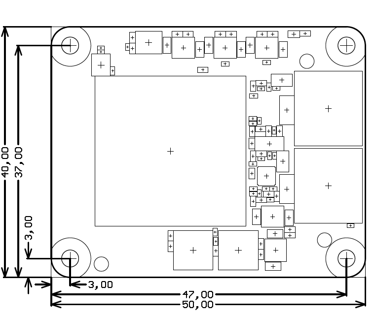
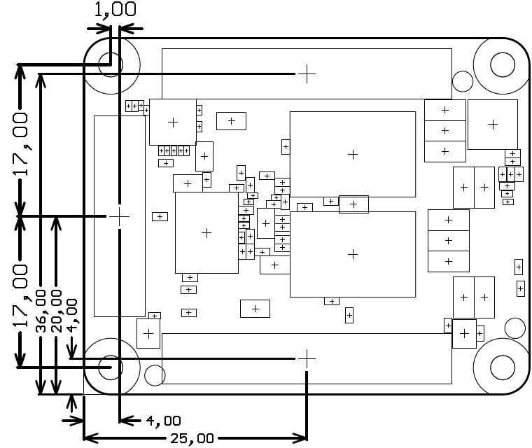
Figure 3: Module physical dimensions.
Weight
47 g - Plain module.
...
Hardware revision number is printed on the PCB board together with the module model number separated by the dash.
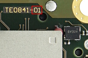
Figure 4: Module hardware revision number.
Document Change History
Date | Revision | Contributors | Description | ||||||||
|---|---|---|---|---|---|---|---|---|---|---|---|
| Jan Kumann | Initial document. |
...
Overview
Content Tools