Page History
...
Technical Specifications
Absolute Maximum Ratings
Parameter | Min | Max | Units | Reference Document |
|---|---|---|---|---|
VIN supply voltage |
| -0.3 | 7.0 | V | EN63A0QI, TPS82085SIL datasheets. | |
| 3.3VIN supply voltage | -0.1 | 3.75 | V | TPS27082, LCMXO2-256HC datasheets. |
| Supply voltage for HR I/O banks (VCCO) | –0.500 | 3.400 | V |
| Xilinx datasheet DS892. | |||
Supply voltage for HP I/O banks (VCCO) | –0.500 | 2.000 | V |
| Xilinx datasheet DS892. | |||
| I/O input voltage for HR I/O banks | –0.400 | VCCO + 0.550 | V |
| Xilinx datasheet DS892. | |||
I/O input voltage for HP I/O banks | –0.550 | VCCO + 0.550 | V |
| Xilinx datasheet DS892. | |||
| GTH and GTY transceiver reference clocks absolute input voltage (MGT_CLK0, MGT_CLK2) | -0.500 | 1.320 | V |
| Xilinx datasheet DS892. | |||
GTH and GTY transceiver receiver (RXP/RXN) and transmitter (TXP/TXN) absolute input voltage | -0.500 | 1.260 | V |
| Xilinx datasheet DS892. | ||||
Storage temperature | -40 | +85 | °C | - |
Table 14: Module absolute maximum ratings.
Recommended Operating Conditions
| Parameter | Min | Max | Units | Reference Document |
|---|---|---|---|---|
| VIN supply voltage |
| 2.5 | 6.0 | V | TPS82085SIL datasheet. | |
| 3.3VIN supply voltage | 2.375 | 3.6 | V | LCMXO2-256HC datasheet. |
| Supply voltage for HR I/O banks (VCCO) | 1.140 | 3.400 | V |
| Xilinx datasheet DS892. | |||
Supply voltage for HP I/O banks (VCCO) | 0.950 | 1.890 | V |
| Xilinx datasheet DS892. | |||
I/O input voltage | –0.200 | VCCO + 0.20 | V |
| Xilinx datasheet DS892. |
Table 15: Module recommended operating conditions.
...
All dimensions are given in millimeters.
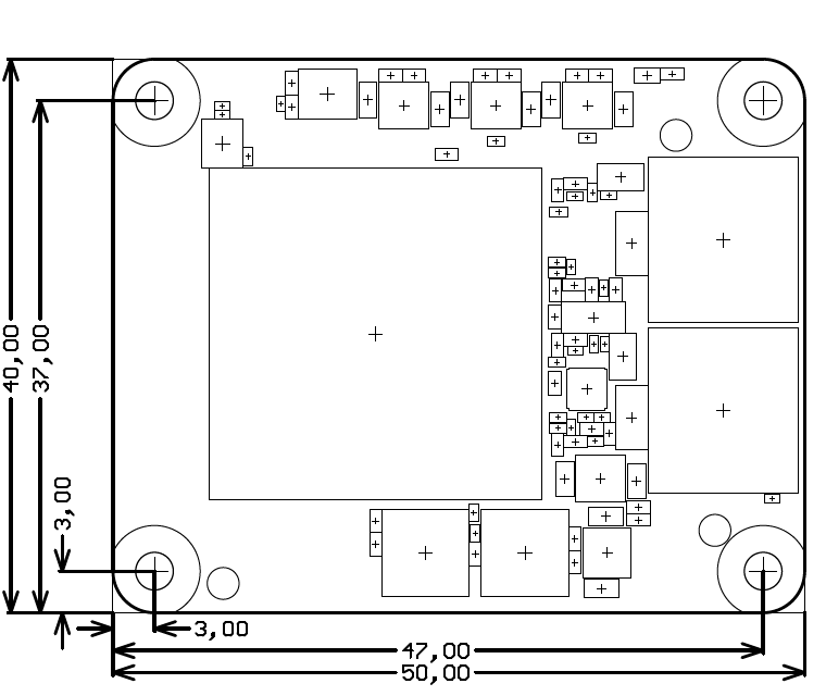
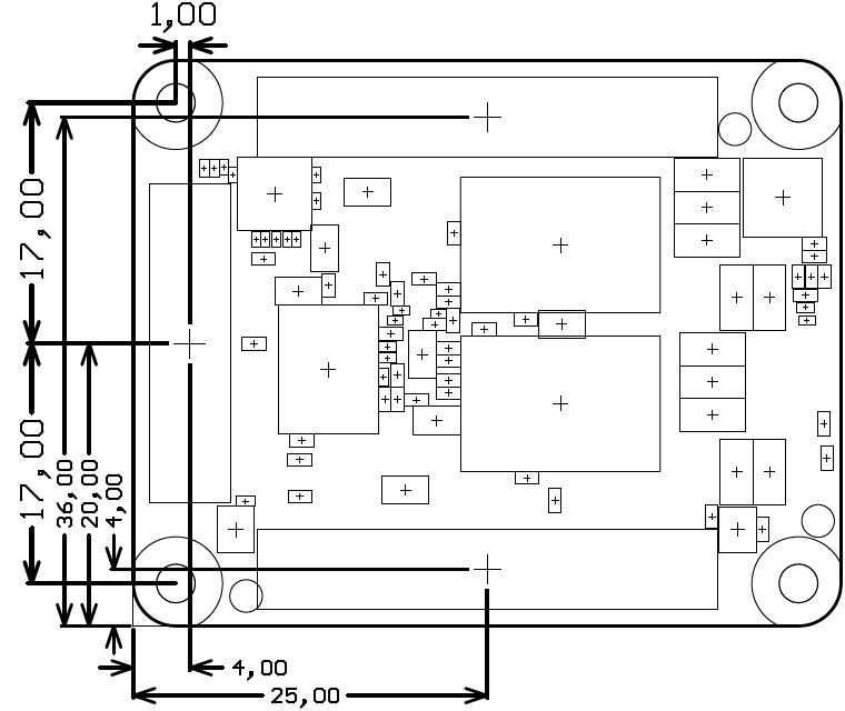
Figure 3: Module physical dimensions.
...
Overview
Content Tools