Page History
...
Figure 1: TEBF0808-04 Block Diagram
Block Diagram description of depicted on-board peripherals
| On-board Peripheral | B2B Connector | MPSoC Unit / SoM peripheral | Description | TRM Section |
|---|---|---|---|---|
| FMC HPC J5, 24 LVDS pairs (48 I/O's) | J1 | PL Bank (FMC_VADJ) | PL I/O-bank pins, differential pairs | |
| FMC HPC J5, GTH Interface | J1 | MGT Bank | 10 MGT Lanes | |
| SFP+ 2x1 Cage J14 | J1 | MGT Bank | 2 MGT Lanes to dual SFP+ Connector | |
| SMA Coax J33 | J1 | On-module PLL | SMA Coaxial Connector to on-module PLL Clock Input pin | |
FMC HPC J5
| J2 | PL Bank (FMC_VADJ) MGT Bank | PL I/O-bank pins, differential pairs 1 clock capable PL bank pin-pair 2 MGT clock input pin-pairs | |
| 24-bit Audio Codec U3 | J3 | PL Bank (1.8 V) | PL I/O-bank pins to on-board 24-bit Audio Codec | |
| 10 I/O's to SC CPLD U17 | J3 | PL Bank (1.8 V) | PL I/O-bank pins to on-board | |
| 8 I/O's to SC CPLD U39 | J3 | PL Bank (1.8 V) | PL I/O-bank pins to on-board | |
| SDIO Interface, SD- / MMC-Card Mux | J3 | PS MIO | SDIO interface connected to SD- / MMC-Card socket | |
| Board Peripheral's I²C Interfaces muxed to MPSoC I²C | J3 | PS MIO | MPSoC I²C interface configured as master connected to on-board slaves | |
| 4 MIO to SC CPLD U17 | J3 | PS MIO | Functionality depending on MPSoC and CPLD firmware | |
| 15 MIO to SC CPLD U39 | J3 | PS MIO | Functionality depending on MPSoC and | |
| Ethernet PHY RGMII | J3 | PS MIO | Ethernet PHY U12 connected per RGMII | |
| eMMC Flash | J3 | PS MIO | eMMC Flash memory interface on PS bank | |
| USB2.0 PHY ULPI | J2 | PS MIO | USB2.0 PHY U9 connected per ULPI | |
| SAMTEC FireFly Connector J6/J15 | J2 | MGT Bank | MGT Lanes to Samtec FireFly connector | |
| JTAG Interface via XMOD Header J12 | J2 | PS Config | MPSoC USB programmable JTAG interface | |
| USB3.0 Lane | J2 | PSGT | USB3.0 PS MGT Lane | |
| 4-port USB3.0 Hub | - | - | USB3.0 (2.0 compatible) Hub with 4 ports | |
| USB3.0 / RJ45 GbE Connector J7, USB3.0 Connector J8 | - | - | 2-port USB3.0 / RJ45 GbE Connector (stacked) | |
| 25 SoM Control Signals to SC CPLDs U17 / U39 | J2 | On-module DC-DC converter, PLL clock generator | Control Signals, e.g. "Enable"- / "Power Good"- signals of DC-DC-converter and further on-module peripherals | |
| 150 MHz Osci Clock Input | J2 | - | 150 MHz SATA interface MGT clock | |
Signals DONE, INIT_B, SRST_B, ... | J2 | PS Config | MPSoC control signal for PS- / PL configuration | |
SATA Connector J31 | J2 | PSGT | Connectors of the MGT based data interfaces | |
PLL Clock Output to
| J2 | On-module PLL clock generator | Reference clock signals of the on-module | |
| 4 I/O's to PMOD P2 via IC U33 | J4 | PL Bank (FMC_VADJ) | PL user I/O's accessible on PMOD connector P2 | |
| 3 I/O's to SC CPLD U17 via IC U32 | J4 | PL Bank (FMC_VADJ) | PL user I/O's routed to System Controller CPLD U17 | |
FMC HPC J5
| J4 | PL Bank (FMC_VADJ) | PL I/O-bank pins, differential pairs 1 clock capable PL bank pin-pair |
Table 1: Description of depicted on-board peripherals
Main Components
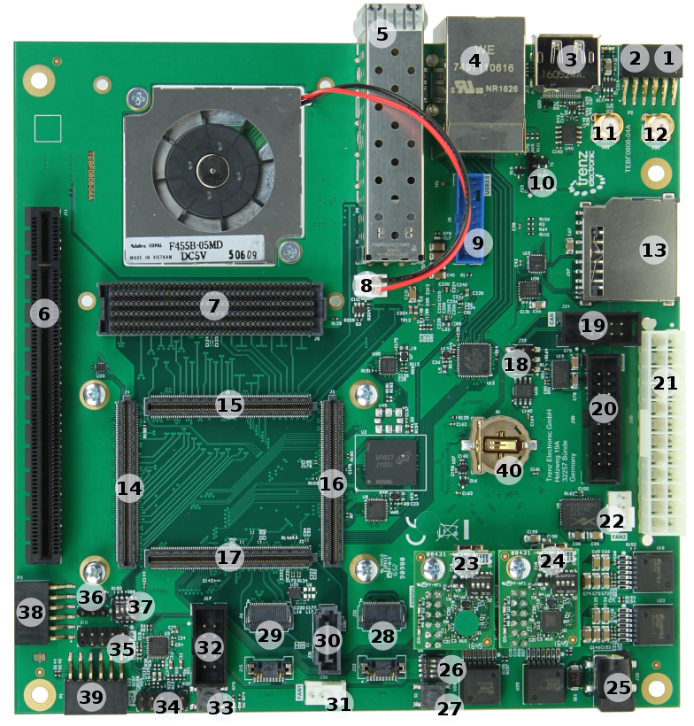
Figure 2: TEBF0808-04 Carrier Board
...
Overview
Content Tools