Page History
...
* TBD - To be determined.
Power-On Sequence
For the highest efficiency of the on-board DC-DC regulators, it is recommended to use same one 3.3V power source for both VIN and 3.3VIN power rails. Although VIN and 3.3VIN can be powered up in any order, it is recommended to power them up simultaneously. It is important that all baseboard I/Os of the carrier board are 3-stated at the beginning of the power-on until System Controller CPLD sets PGOOD signal high (B2B connector JM1, pin 30), or cycle until 3.3V is present on B2B connector JM2 pins 10 and 12, meaning indicating that all on-module PL supply voltages have become stable and Zynq MPSoC module is properly powered up properly.
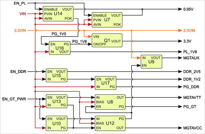
Figure 3: TE0841-01 Power-on sequence.
See also Xilinx datasheet DS892 for additional information. User should also check related baseboard documentation when choosing baseboard design for TE0720 module.
Figure 3: TE0841-01 Power-on sequenceTE0841 module.
Power Rails
| Power Rail Name | B2B JM1 Pins | B2B JM2 Pins | Input/Output | Notes |
|---|---|---|---|---|
| VIN | 1, 3, 5 | 2, 4, 6, 8 | Input | Supply voltage. |
| 3.3VIN | 13, 15 | - | Input | Supply voltage. |
| B64_VCO | 9, 11 | - | Input | HR (High Range) bank voltage. |
| B66_VCO | - | 1, 3 | Input | HP (High Performance) bank voltage. |
| B67_VCO | - | 7, 9 | Input | HP (High Performance) bank voltage. |
| B68_VCO | - | 5 | Input | HP (High Performance) bank voltage. |
VBAT_IN | 79 | - | Input | RTC battery supply voltage. |
| 3.3V | - | 10, 12, 91 | Output | Module on-board 3.3V voltage level. |
...
Overview
Content Tools