Page History
...
Table 12: Pin description of PLL clock generator Si5338A
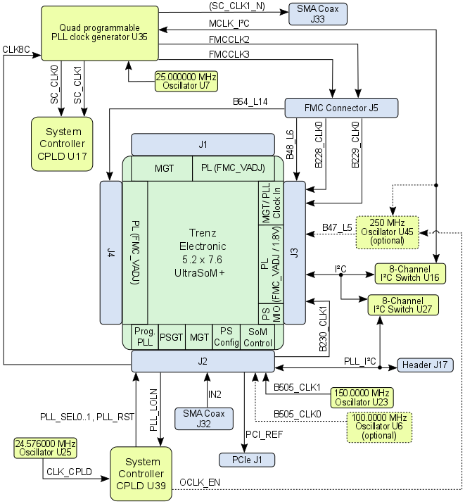
Figure 11: Clocking Configuration of TE0808 SoM on TEBF0808 Carrier Board
...
The power-on sequence of the TE0808 SoM is managed by utilizing the SoM's DC-DC converter control signals ('Enable', 'Power-Good'), so the DC-DC converters of the SoM dedicated to the particular Power Domains of the Zynq Ultrascale+ MPSoC will be powerer-up in a specific sequence to meet the recommended criteria to power up the Xilinx Zynq Ultrascale+ MPSoC properly.
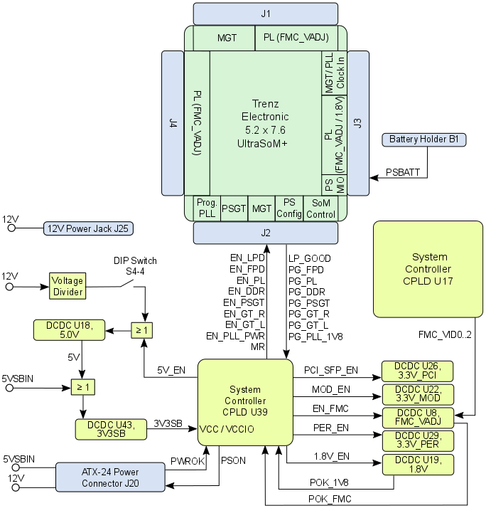
Figure 12: TEBF0808 Power-Management
Adjustable PL Bank VCCO Voltage FMC_VADJ
The carrier board VCCO voltage 'FMC_VADJ' supplying the PL IO-banks of the MPSoC (bank 64, 65, 66, 48) is provided by DC-DC converter U8 and selectable by the pins 'FMC_VID0' ... 'FMC_VID2' of the System Controller CPLD U17.
...
FMC_VADJ Value
...
On Sequence Utilizing DCDC Converter Control Signals
| Warning |
|---|
| To avoid any damages to the MPSoC module, check for stabilized on-board voltages in steady state before powering up the MPSoC's I/O bank voltages VCCOx. All I/O's should be tri-stated during power-on sequence. |
Core voltages and main supply voltages of the Zynq Ultrascale+ MPSoC have to reach stable state and the "Power Good"-signals of the SoM have to be asserted before other voltages like bank's I/O voltages (VCCOx) can be powered up.
It is important that all PS and PL I/Os are tri-stated at power-on until the "Power Good"-signals are logically high, meaning that all on-module voltages have become stable and module is properly powered up.
Adjustable PL Bank VCCO Voltage FMC_VADJ
The carrier board VCCO voltage 'FMC_VADJ' supplying the PL IO-banks of the MPSoC (bank 64, 65, 66, 48) is provided by DC-DC converter U8 and selectable by the pins 'FMC_VID0' ... 'FMC_VID2' of the System Controller CPLD U17.
| FMC_VID2 | FMC_VID1 | FMC_VID0 | FMC_VADJ Value |
|---|---|---|---|
| 0 | 1 | 0 | 1.8V |
| 0 | 1 | 1 | 1.5V |
| 1 | 0 | 0 | 1.25V |
| 1 | 0 | 1 | 1.2V |
Table 3: Bit patterns for fixed values of the FMC_VADJ voltage
Note: These pins of the DC-DC converter U8 are hard-wired to initialiy fix the voltage to 1.8V (see schematic).
Power Distribution Dependencies
All on-board voltages of the TEBF0808 are generated out of the extern applied 12V power supply.
There are following dependencies how the initial 12V power supply is distributed to the on-board DC-DC converters, which power up further DCDC converters and the particular on-board voltages:
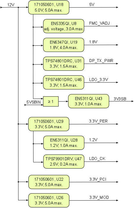
Figure 13: Power Distribution Diagram
| Note |
|---|
Current rating of Samtec Razor Beam™ LSHM B2B connectors is 2.0A per pin (2 adjacent pins powered). |
Table 3: Bit patterns for fixed values of the FMC_VADJ voltage
Note: These pins of the DC-DC converter U8 are hard-wired to initialiy fix the voltage to 1.8V (see schematic).
Power Distribution Dependencies
All on-board voltages of the TEBF0808 are generated out of the extern applied 12V power supply.
There are following dependencies how the initial 12V power supply is distributed to the on-board DC-DC converters, which power up further DCDC converters and the particular on-board voltages:
Figure 13: Power Distribution Diagram
| Note |
|---|
Current rating of Samtec Razor Beam™ LSHM B2B connectors is 2.0A per pin (2 adjacent pins powered). |
Power-On Sequence Diagram
The power-on sequence of the on-board DC-DC converters depens on the current firmware of the System Controller CPLD U17.
Following diagram visualizes the connection of the DC-DC converter control signals ('Enable', 'Power-Good') with System Controller CPLD U17, which enables the particular on-board voltages.
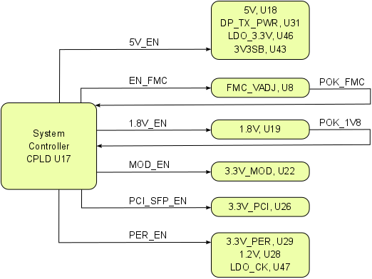
Figure 14: Power-On Sequence Utilizing DCDC Converter Control Signals
| Warning |
|---|
| To avoid any damages to the MPSoC module, check for stabilized on-board voltages in steady state before powering up the MPSoC's I/O bank voltages VCCOx. All I/O's should be tri-stated during power-on sequence. |
Core voltages and main supply voltages of the Zynq Ultrascale+ MPSoC have to reach stable state and the "Power Good"-signals of the SoM have to be asserted before other voltages like bank's I/O voltages (VCCOx) can be powered up.
It is important that all PS and PL I/Os are tri-stated at power-on until the "Power Good"-signals are logically high, meaning that all on-module voltages have become stable and module is properly powered up.
B2B connectors
| Include Page | ||||
|---|---|---|---|---|
|
...
Overview
Content Tools