Page History
...
Figure 3: TE0722-02 PCB bottom side.
- Xilinx Zynq XC7Z010 or Zynq XC7Z007S SoC, U1
- Micro SD card socket with card detect, J8
- Red LED, D3
- Green LED, D2
- Red LED, D6
- 20-pin connector placeholder, P1
- Red LED, D5
- Proximity/ambient light sensor, U4
- RGB LED, D4
- Red LED, D1
- 20-pin connector placeholder, P2
- Ultra-low supply-current voltage monitor, U4
- 2 x 5-pin connector placeholder, J1
- 2 x 5-pin connector placeholder, J2
- 2 x 5-pin connector placeholder, J3
- 16 MByte QSPI Flash memory, U5
- Low power programmable oscillator @ 33.333333 MHz, U8
- 1A PowerSoC DC-DC converter (1.0V), U2
- 1A PowerSoC DC-DC converter (1.8V), U3
...
I/O Signals
Overview of the signals between PL I/O banks and signals routed to the external connectors:
| Bank | Type | Connector | I/O Signal Count | Voltage | Notes |
|---|---|---|---|---|---|
| 34 | HR | P1 | 8 | 3.3 | P0 - P7 |
| 34 | HR | P2 | 8 | 3.3 | P24 - P31 |
| 34 | HR | P2 | 10, 5 LVDS pairs | 3.3 | |
| 34 | HR | J1 | 6 | 3.3 | X2A - X2F |
| 34 | HR | J2 | 2 | 3.3 | |
| 34 | HR | J3 | 4 | 3.3 | X1A - X1D |
| 35 | HR | P1 | 8, 4 LVDS pairs | 3.3 |
Table 3: PL I/O signals overview.
JTAG Interface
JTAG access to the Xilinx ZYNQ XC7Z010 SoC is provided through J2 connector.
JTAG Signal | J2 Connector Pin |
|---|---|
| TCK | 4 |
| TDI | 9 |
| TDO | 10 |
| TMS | 8 |
Table 4: JTAG interface signals.
Default PS MIO Mapping
| MIO | Function | Connector Pin | Notes |
|---|---|---|---|
| 0 | - | - | - |
| 1 | QSPI | - | SPI Flash-CS |
| 2 | QSPI | - | SPI Flash-DQ0 |
| 3 | QSPI | - | SPI Flash-DQ1 |
| 4 | QSPI | - | SPI Flash-DQ2 |
| 5 | QSPI | - | SPI Flash-DQ3 |
| 6 | QSPI | - | SPI Flash-SCK |
| 7 | GPIO | - | Green LED D2 |
| 8 | - | - | - |
| 9 | - | - | - |
| 28 | SD CARD | J8-5 | CLK |
| 29 | SD CARD | J8-3 | CMD |
| 30 | SD CARD | J8-7 | DAT0 |
| 31 | SD CARD | J8-8 | DAT1 |
| 32 | SD CARD | J8-1 | DAT2 |
| 33 | SD CARD | J8-2 | CD/DAT3 |
| 36 | I2C | - | SCL |
| 37 | I2C | - | SDA |
| 39 | GPIO | - | Si1143 INT pin |
| 49 | SD CARD | J8-G4 | Card detect switch |
...
Power supply with minimum current capability of 1A for system startup is recommended.
Power-On Sequence
... diagram will be here soon ...
Variants Currently in Production
| Module Variant | Xilinx Zynq SoC | ARM Cortex-A9 Cores | PL Cells | LUTs | Flip-Flops | Block RAM | DSP Slices | Operating Temperature | Temperature Range |
|---|---|---|---|---|---|---|---|---|---|
| TE0722-02I | XC7Z010-1CLG225I | Dual-core ARM Cortex-A9 | 28K | 17,6K | 35,2K | 2.1 MBytes | 80 | –40°C to +85°C | Industrial |
| TE0722-02 | XC7Z010-1CLG225I1CLG225C | Dual-core ARM Cortex-A9 | 28K | 17,6K | 35,2K | 2.1 MBytes | 80 | 0°C to +70°C | Commercial |
| TE0722-02-07S-1C | XC7Z007S-1CLG225C | Single-core ARM Cortex-A9cor | 23K | 14,4K | 28,8K | 1.8 MBytes | 66 | 0°C to +70°C | Commercial |
Table 8: Module variants.
...
Hardware revision number is printed on the PCB board together with the module model number separated by the dash.
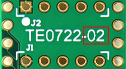
Figure 5: TE0722 module hardware revision number.
Document Change History
Date | Revision | Contributors | Description | ||||||||
|---|---|---|---|---|---|---|---|---|---|---|---|
| Jan Kumann | Initial document. |
Table 12: Document change history..
Disclaimer
| Include Page | ||||
|---|---|---|---|---|
|
Overview
Content Tools