Page History
...
| Scroll Only (inline) |
|---|
Refer to "https://shopwiki.trenz-electronic.de/endisplay/Download/?path=Trenz_Electronic/TE0808"PD/TE0808+TRM for downloadable version of this manual and the rest of available documentation. |
The Trenz Electronic TE0808 is an industrial-grade MPSoC SoM integrating a Xilinx Zynq UltraScale+ MPSoC, max. 8 GByte up to 8 GBytes of DDR4 SDRAM with via 64-Bit width databus connectionbit wide data bus, max. 512 MByte Flash memory for configuration and operation, 20 Gigabit transceivers and powerful switch-mode power supplies for all on-board voltages. A large number of configurable I/O's is Os are provided via rugged high-speed stacking connections. All this in a compact 5.2 x 7.6 cm form factor, at the most competitive price.
| Note |
|---|
Important Information for TE0808 boards which are equipped with ES1 or ES2 silicon: Erratas and functional restrictions may exist, please check Xilinx documentation and contact your local Xilinx FAE for restrictions. |
...
- MPSoC: ZYNQ UltraScale+ ZU9EG 900 pin package
- Memory
- 64-Bit DDR4, 8 GByte maximum
- Dual SPI boot Flash in parallel, 512 MByte maximum - User I/OOs
- 65 x MIOPS MIOs, 48 x PL HD (all)GPIOs, 156 x PL HP GPIOs (3 banks)
- Serial transceivertransceivers: 4 x GTR + 16 x GTH
- Transceiver clocks inputs and outputs
- PLL clock generator inputs and outputs - Size: 52 x 76 mm, 3 mm mounting holes for skyline heat spreader
- B2B connectors: 4 x 160 pin
- Si5345 - 10 output PLL
- All power supplies on board, single 3.3V power source required
- 14 on-board DC-DC regulators and 13 LDOs
- LP, FP, PL separately controlled power domains - Support for all boot modes (except NAND) and scenarios
- Support for any combination of PS connected peripherals
- Size: 52 x 76 mm, 3 mm mounting holes for skyline heat spreader
- B2B connectors: 4 x 160 pin
Block Diagram
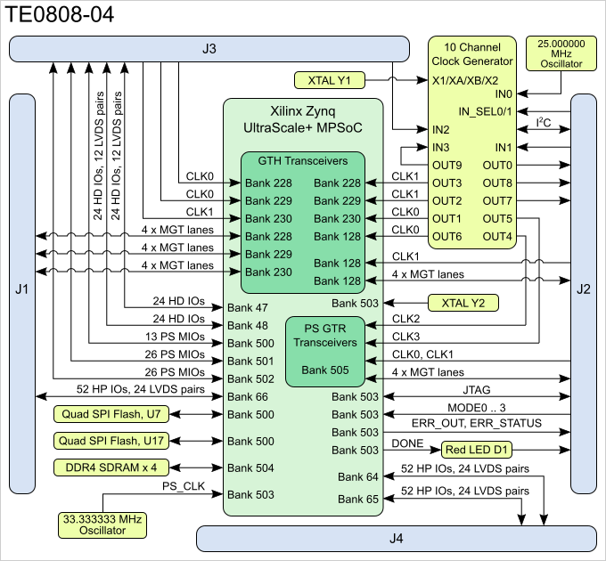
Figure 1: TE0808-04 Block Diagram.
...
- Xilinx ZYNQ UltraScale+ XCZU9EG MPSoC, U1
- Low-power programmable oscillator @ 33.333333 MHz (PS_CLK), U32
- Red LED (DONE), D1
- 256Mx16 DDR4-2400 SDRAM, U12
- 256Mx16 DDR4-2400 SDRAM, U9
- 256Mx16 DDR4-2400 SDRAM, U2
- 256Mx16 DDR4-2400 SDRAM, U3
- 12A PowerSoC DCDC DC-DC converter, U4
- Quartz crystal, Y1
- Low-power programmable oscillator @ 25.000000 MHz (IN0 for U5), U25
- 10-channel programmable PLL clock generator, U5
- Ultra fine 0.50 mm pitch, Razor Beam™ LP Slim Terminal Strip with 160 contacts, J4
- Ultra fine 0.50 mm pitch, Razor Beam™ LP Slim Terminal Strip with 160 contacts, J2
- Ultra fine 0.50 mm pitch, Razor Beam™ LP Slim Terminal Strip with 160 contacts, J3
- Ultra fine 0.50 mm pitch, Razor Beam™ LP Slim Terminal Strip with 160 contacts, J1
- Quartz crystal, Y2
- 256 Mbit serial NOR Flash memory, U7
- 256 Mbit serial NOR Flash memory, U17
...
Each connector has a specific arrangement of the signal pins, which are grouped together in categories related to their functionalities and to their belonging to particular units of the Zynq UltrascaleUltraScale+ MPSoC like I/O - banks, interfaces and Gigabit transceivers
or to the on-board peripherals.
...
| Bank | Type | B2B Connector | Schematic Names / Connector Pins | I/O Signal CountSignals | LVDS Pairs Count | VCCO Bank Voltage | Notes |
|---|---|---|---|---|---|---|---|
| 47 | HD | J3 | B47_L1_P ... B47_L12_P | 24 I/O'sOs | 12 | VCCO47 | VCCO max. 3.3V |
| 48 | HD | J3 | B48_L1_P ... B48_L12_P | 24 I/O'sOs | 12 | VCCO48 | VCCO max. 3.3V |
| 64 | HP | J4 | B64_L1_P ... B64_L24_P B_64_T0 ... B_64_T3 | 52 I/O's | 24 | VCCO64 | VCCO max. 1.8V |
| 65 | HP | J4 | B65_L1_P ... B65_L24_P B_65_T0 ... B_65_T3 | 52 I/O'sOs | 24 | VCCO65 | VCCO max. 1.8V |
| 66 | HP | J1 | B66_L1_P ... B66_L24_P B_66_T0 ... B_66_T3 | 48 I/O'sOs | 24 | VCCO66 | VCCO max. 1.8V |
| 500 | MIO | J3 | MIO13 ... MIO25 | 13 I/O'sOs | - | PS_1V8 | user User configurable I/O's Os on B2B |
| 501 | MIO | J3 | MIO26 ... MIO51 | 26 I/O'sOs | - | PS_1V8 | user User configurable I/O's Os on B2B |
| 502 | MIO | J3 | MIO52 ... MIO77 | 26 I/O'sOs | - | PS_1V8 | user User configurable I/O's Os on B2B |
Table 2: B2B connector pin-outs of available PL and PS banks of the TE0808-04 SoM.
...
JTAG access is provided through the MPSoC's PS configuration bank 503 with bank voltage ' PS_1V8'.
| JTAG Signal | B2B Connector Pin |
|---|---|
| TCK | J2-120 |
| TDI | J2-122 |
| TDO | J2-124 |
| TMS | J2-126 |
...
The Xilinx Zynq UltraScale+ MPSoC's PS configuration bank 503 control signal pins are accessible through B2B - connector J2.
For further information about the particular control signals and how to use and evaluate them, refer to the Xilinx Zynq UltraScale+ MPSoC TRM and UltraScale Architecture Configuration - User Guide.
| Signal | B2B Connector Pin | Function |
|---|---|---|
| DONE | J2-116 | PL configuration completed. |
| PROG_B | J2-100 | PL configuration reset signal. |
| INIT_B | J2-98 | PS is initialized after a power-on reset. |
| SRST_B | J2-96 | System reset. |
| MODE0 ... MODE3 | J2-109/J2-107/J2-105/J2-103 | 4-bit boot mode pins. For further information about the boot - modes refer to the Xilinx Zynq UltraScale+ MPSoC TRM |
| ERR_STATUS / ERR_OUT | J2-86 / J2-88 | ERR_OUT signal is asserted for accidental loss of power, an error, or an exception in the MPSoC's Platform Management Unit (PMU)-. ERR_STATUS indicates a secure lock-down state. |
| PUDC_B | J2-127 | Pull-up during configuration (pulled-up to PL_1V8). |
...
Quad SPI Flash memory ICs U7 and U17 are connected to the Zynq MPSoC PS QSPI0 interface via PS MIO bank 500, pins MIO0 ... MIO5 and MIO7 ... MIO12.
| MIO | Signal Schematic Name | U7 Pin | MIO | Signal Schematic Name | U17 Pin | |
|---|---|---|---|---|---|---|
| 0 | SPI Flash -SCK/M4CLK | B2 | 7 | SPI Flash -SCKCS | C2 | |
| 1 | SPI Flash-DQ1/M1Flash IO1 | D2 | 8 | SPI Flash -DQ0/M0IO0 | D3 | |
| 2 | SPI Flash -DQ2/M2IO2 | C4 | 9 | SPI Flash -DQ1/M1IO1 | D2 | |
| 3 | SPI Flash -DQ3/M3IO3 | D4 | 10 | SPI Flash -DQ2/M2IO2 | C4 | |
| 4 | SPI Flash -DQ0/M0IO0 | D3 | 11 | SPI Flash -DQ3/M3IO3 | D4 | |
| 5 | SPI Flash -SCKCS | C2 | 12 | SPI Flash -SCK/M4CLK | B2 |
Table 7: PS MIO pin assignment of the Quad SPI Flash memory ICs.
Boot Process
The boot source device and mode of the Zynq UltraScale+ MPSoC can be selected via 4 dedicated pins , which generate a 4-bit code to select the boot mode. The pins are accessible on B2B connector J2:
...
Table 8: Boot mode pins on B2B connector J2.
Following boot modes are possible on the TE0808 UltraScale+ module by generating the corresponding 4-bit code by the pins ' PS_MODE0 ' ... ' PS_MODE3 ' (little-endian alignment):
...
For functional details see ug1085 - Zynq UltraScale+ TRM (Boot Modes Section).
...
| Date | Revision | Contributors | Description | ||||||||||
|---|---|---|---|---|---|---|---|---|---|---|---|---|---|
| Jan Kumann |
| |||||||||||
| 2017-08-15 | v.12 | Vitali Tsiukala | Changed signals count in the B2B connectors table | ||||||||||
| 2017-08-15 | v.11 | John Hartfiel, Ali Naseri |
| ||||||||||
| 2017-02-06 | V1 | Jan Kumann | Initial document |
...
Overview
Content Tools