Page History
...
| Scroll pdf ignore | |
|---|---|
Table of Contents
|
Overview
| Scroll Only (inline) |
|---|
Refer to https://shop.trenz-electronic.de/de/Download/?path=Trenz_Electronic/XMOD/TE0790 for downloadable version of this manual and additional technical documentation of the product. |
...
The board is equipped with a programmable System Controller CPLD provided by Lattice Semiconductor LCMXO2-256HC (MachXO2 Product Family) to control the signals of the serial interfaces. The data stream of the USB2.0 port can be also converted to 8 independent GPIO's or used as FIFO.
Key Features
- Xmod form-factor
- size: 20 x 25 mm
- M3 mounting hole
- FT2232H
- USB2.0 port High Speed (480 Mbps) and Full Speed (12 Mbps) compatible
- Entire USB protocol handled on the chip
- USB2.0 to JTAG, SPI and I²C conversion provided by the IC's Multi-Protocol Synchronous Serial Engine (MPSSE)
- USB2.0 to UART conversion
- Channel B UART RX/TX LED's
- Mini-USB B connector (more rigid then micro-USB)
- 93C56 EEPROM
- Lattice XO2-256 CPLD
- on board programmable using Lattice tools
- 8 universal I/O pins
- VCCIO either 3.3V or user supplied (1.8 to 3.3V)
- RED user LED
- 12 MHz clock from on-board Oscillator
- LDO DCDC for optional USB power
- GREEN Power-on LED
- User button
- 4 position DIP switch
- Choose CPLD program mode
- FTDI EEPROM disable (not implemented in PCB REV 1)
- Use VIO same as VCC
- Use VCC from USB
Block Diagram
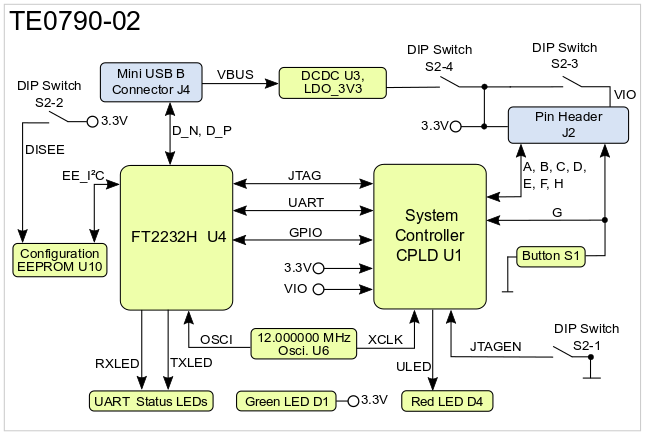
Figure 1: TE0790-02 block diagram.
Main Components
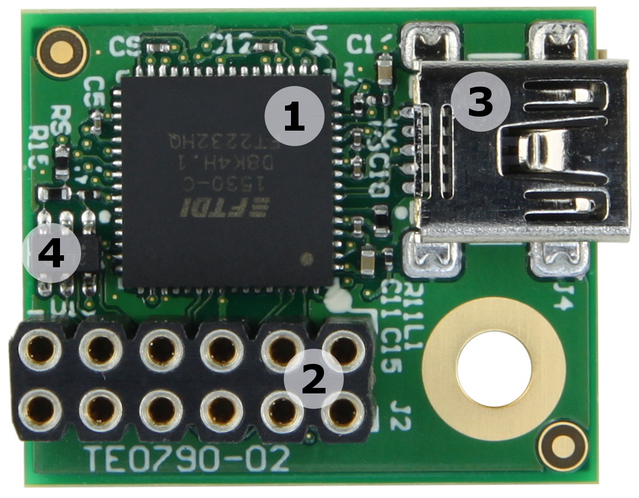
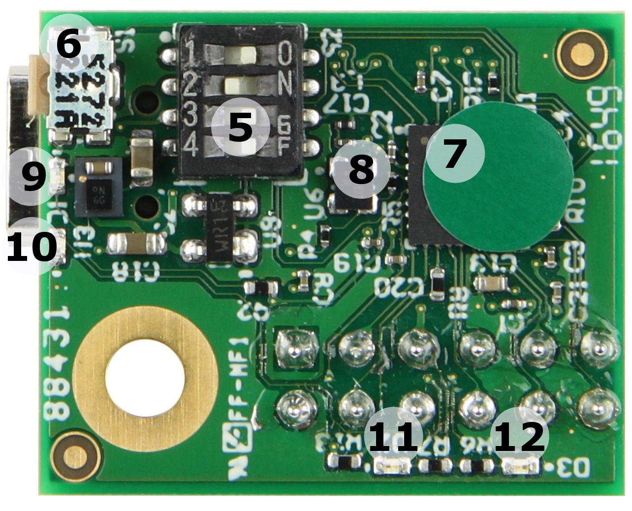
Figure 2: TE0790-02 main components.
- FTDI FT2232H IC U4
- 2x6 Pin Header (2.54mm, female), J2
- Mini USB B Connector J4
- Microchip 93AA56BT-I/OT Configuration EEPROM, U10
- DIP-switch S2
- Push button S1
- Lattice Semiconductor LCMXO2-256HC System Controller CPLD, U1
- SiTime SiT8008AI-73 oscillator @12MHz, U6
- Green LED, D1 (Power)
- Red LED, D4 (User)
- Red LED, D3 (UART RX)
- Red LED, D2 (UART TX)
Initial Delivery State
Storage device name | Content | Notes |
|---|---|---|
| Configuration EEPROM U10 | variant depending | only programmed on TE-0790-xxL variants. |
Table 1: Initial delivery state of programmable devices on the module.
Signals, Interfaces and Pins
2x6 Pin Header
The 2x6 pin header (2.54mm grid size, female) J2 have to be connected to the corresponding pin header on the target system. The signal assignment of the pin header on the adapter board depends on the configuration of the System Controller CPLD firmware.
...
Table 5: Pin header J2 signal assignment with DIPFORTy firmware.
USB Interface
The USB2.0 interface is provided by the FTDI FT2232H chip accessible by the Mini-USB B connector J4. The entire USB protocol is handled on chip and compatible to USB2.0 High Speed (480 MBps) and Full Speed (12 MBps).
On-board Peripherals
FTDI FT2232H IC
The FTDI FT2232H chip provides a variety of industry standard serial or parallel interfaces. On the TE0790 adapter board at current available SC CPLD firmware the functions USB2.0 to JTAG, UART and user GPIO's.
By programing the firmware of the SC CPLD and special EEPROM configurations further further functionalities are available of the FTDI chip which converts signals from USB2.0 to a variety of standard serial and parallel interfaces. Refer to the FTDI data sheet to get information about the capacity of the FT2232H IC.
Configuration EEPROM
In order to work with Xilinx tools special order must be used, in that case the EEPROM is pre-programmed and serialized and will be recognized by all Xilinx tools (ISE/Impact/Chipscope, Vivado Programmer/SDK..).
| Warning |
|---|
Do not access the FT2232H EEPROM using FTDI programming tools, doing so will erase normally invisible user EEPROM content and invalidate stored Xilinx JTAG license. Without this license the on-board JTAG will not be accessible any more with any Xilinx tools. Software tools from FTDI website do not warn or ask for confirmation before erasing user EEPROM content. |
System Controller CPLD
The System Controller CPLD (U1) is provided by Lattice Semiconductor LCMXO2-256HC (MachXO2 Product Family). The SC-CPLD is the central system management unit where essential control signals are logically linked by the implemented logic in CPLD firmware, which generates output signals to control the system, the on-board peripherals and the interfaces.
...
The internal routing of the signals between the USB2.0 interface and pin header J2 on the System Controller CPLD depends on its configured firmware. Refer to the Resources Site of the TE0790 for more information about the currently available System Controller CPLD firmware and for download.
DIP-switch
The DIP-switch S2 is to set different modes of powering the on-board peripherals and their I/O supply voltages.
...
Table 7: DIP-switch S2 power setting description.
User Push Button
The user push button S1 directly connected to the SC CPLD manipulates pin G of the pin header J2 by driving it to GND.
On-board LEDs
The on-board LEDs indicates system status data transmission activities:
| LED | Color | Connected to | Description and Notes |
|---|---|---|---|
| D1 | Green | 3.3V | 3.3V power status LED |
| D2 | Red | FTDI IC, 'RXLED' | UART receive data activity |
| D3 | Red | FTDI IC, 'TXLED' | UART transmit data activity |
| D4 | Red | SC CPLD, 'ULED' | user LED, on standard SC CPLD firmware assigned to pins E and G, in DIPFORTy to G |
Table 8: On-board LEDs.
Power and Power-On Sequence
Power supply of the adapter board
The adapter on-board's peripherals are powered with 3.3V as supply voltage. If 3.3V (VCC and VIO) is supplied only by the LDO DCDC U3 (S2-3 and S2-4 OFF), the I/O-pins of header J2 deliver max. ~100mA.
If module is powered from base then S2-4 (and most likely S2-3 (VIO) too) must be OFF.
Power Rails
Power Rail Name | Pin Header J2 | Direction | Notes |
|---|---|---|---|
| 3.3V | pin 5 | both possible | user configurable by DIP-switch S2-3 and S2-4 |
| VIO | pin 6 | both possible | user configurable by DIP-switch S2-3 and S2-4 |
Table 9: Module power rails.
Variants Currently In Production
Module Variant | Xilinx Vivado/SDK Support | Xilinx devices with 3rd Party Tools | Any other MPSSE based JTAG Tools |
|---|---|---|---|
| TE0790-02 | Yes | Yes | Yes |
| TE0790-02L | No | Yes | Yes |
...
Variants with TE-0790-xxL do not include the ID String in EEPROM for direct support from Xilinx Vivado.
Technical Specifications
Absolute Maximum Ratings
| Parameter | Min | Max | Units | Reference Document |
|---|---|---|---|---|
3.3V | -0.3 | 4 | V | FTDI FT2232H data sheet |
| VIO | -0.5 | 3.75 | V | Lattice MachX02 Family data sheet |
| Voltage on pins A - H | -0.5 | 3.75 | V | Lattice MachX02 Family data sheet |
| Storage temperature | °C |
Table 11: Module absolute maximum ratings.
Recommended Operating Conditions
| Parameter | Min | Max | Units | Reference Document |
|---|---|---|---|---|
3.3V | V | |||
| VIO | V | |||
| Voltage on pins A - H | V | |||
| Operating temperature | °C |
Table 12: Module recommended operating conditions.
Operating Temperature Ranges
Commercial grade: 0°C to +70°C.
...
Industrial grade: -40°C to +85°C.
Physical Dimensions
Module size: 24,65mm × 20,02mm. Please download the assembly diagram for exact numbers.
Mating height with standard connectors: ... mm.
PCB thickness: ... mm.
Highest part on PCB: approx. ... mm. Please download the step model for exact numbers.
...
Figure 3: Module physical dimensions drawing.
Revision History
Hardware Revision History
| Date | Revision | Notes | PCN | Documentation Link |
|---|---|---|---|---|
| - | 01 | prototypes | - | - |
| - | 02 | current available revision | - | TE0790-02 |
...
Figure 4: Module hardware revision number.
Document Change History
| HTML |
|---|
<!-- Generate new entry: 1.add new row below first 2.Copy "Page Information Macro(date)" Macro-Preview, Metadata Version number, Author Name and description to the empty row. Important Revision number must be the same as the Wiki document revision number 3.Update Metadata = "Page Information Macro (current-version)" Preview+1 and add Author and change description. --> |
...
Table 14: Document change history.
Disclaimer
| Include Page | ||||
|---|---|---|---|---|
|
...
Overview
Content Tools