Page History
...
The board is equipped with a programmable System Controller CPLD provided by Lattice Semiconductor LCMXO2-256HC (MachXO2 Product Family) to control the signals of the configured interfaces. The data stream of the USB2.0 port can be also converted to 8 independent GPIO's or used as FIFO.
Following table describes the possible operation modes of the TE0790 adapter board. The operation modes ared determined by the configuration of the FT2232H, which is done by programing the Configuration EEPROM and the System Controller CPLD:
| # | FTDI Channel A | FTDI Channel B | Pins A to G | Notes |
|---|---|---|---|---|
| 1 | JTAG/SPI (MPSSE) | UART | JTAG, UART | JTAG compatible to Xilinx, Lattice and open-source software that uses FTDI MPPSE |
| 2 | JTAG/SPI (MPSSE) | JTAG/SPI (MPSSE) | JTAG, JTAG | Dual JTAG, only Channel A is Xilinx compatible |
| 3 | UART | UART | UART, UART | Dual UART |
| 4 | I2C | UART | I2C, UART | |
| 5 | MPSSE | 8x GPIO | ||
| 6 | UART | 8x GPIO | ||
| 7 | UART | UART | not used | UART to UART loopback |
| 8 | not used | Fast Serial | FTDI 4-wire fast serial adapter, custom EEPROM is needed to enable this mode | |
| 9 | CPLD update only | not used | user defined | Standalone Module with CPLD and 8 user programmable I/O |
Table 1: Initial delivery state of programmable devices on the module.
MPSSE - FTDI protocol that is used by JTAG and SPI adapters based on FTDI devices.
Key Features
- Xmod form-factor
- size: 20 x 25 mm
- M3 mounting hole
- FT2232H
- USB2.0 port High Speed (480 Mbps) and Full Speed (12 Mbps) compatible
- Entire USB protocol handled on the chip
- USB2.0 to JTAG, SPI and I²C conversion provided by the IC's Multi-Protocol Synchronous Serial Engine (MPSSE)
- USB2.0 to UART conversion
- Channel B UART RX/TX LED's
- Mini-USB B connector (more rigid then micro-USB)
- 93C56 EEPROM
- Lattice XO2-256 CPLD
- on board programmable using Lattice tools
- 8 universal I/O pins
- VCCIO either 3.3V or user supplied (1.8 to 3.3V)
- RED user LED
- 12 MHz clock from on-board Oscillator
- LDO DCDC for optional USB power
- GREEN Power-on LED
- User button
- 4 position DIP switch
- Choose CPLD program mode
- FTDI EEPROM disable (not implemented in PCB REV 1)
- Use VIO same as VCC
- Use VCC from USB
...
Storage device name | Content | Notes |
|---|---|---|
| Configuration EEPROM U10 | variant depending | only programmed on TE-0790-xx, not programmed on TE0790-xxL variants. |
Table 12: Initial delivery state of programmable devices on the module.
...
| Signal | J2 Pin Name | J2 Pin Name | Signal |
|---|---|---|---|
| GND | 1* | GND | |
| User Defined | C | A | User Defined |
| VIO | VDD 3.3V | ||
| User Defined | D | B | User Defined |
| User Defined | F | E | User Defined |
| User Defined | H | G | User Defined / Button (Reset_n) |
Table 23: Pin header J2 signal assignment. *pin 1 on header J2
The signals of the FTDI FT2232H chip are not directly connected to the pin header J2 but routed to the System Controller CPLD of the adapter board, which controls and by-passes the signals to the pin header J2.
...
| FTDI | Signal | Pull up/down | J2 Pin Name | J2 Pin Name | Pull up/down | Signal | FTDI |
|---|---|---|---|---|---|---|---|
| GND | - | 1* | - | GND | |||
| ADBUS0 | TCK (output from adapter) | C | A | up | UART RXD (input to adapter) | BDBUS1 | |
| VIO | - | - | VDD 3.3V | ||||
| ADBUS2 | TDO (input to adapter) | up | D | B | UART TXD (output from adapter) | BDBUS0 | |
| ADBUS1 | TDI (output from adapter) | F | E | down | LED | ||
| ADBUS3 | TMS (output from adapter) | H | G | up | Button (Reset_n) |
Table 34: Pin header J2 signal assignment with standard configuration firmware. *pin 1 on header J2
Signal assignment on Standard with RXD-TXD Swapped:
...
| FTDI | Signal | Pull up/down | J2 Pin Name | J2 Pin Name | Pull up/down | Signal | FTDI |
|---|---|---|---|---|---|---|---|
| GND | - | 1* | - | GND | |||
| ADBUS0 | TCK (output from adapter) | C | A | UART TXD (output from adapter) | BDBUS0 | ||
| VIO | - | - | VDD 3.3V | ||||
| ADBUS2 | TDO (input to adapter) | up | D | B | up | UART RXD (input to adapter) | BDBUS1 |
| ADBUS1 | TDI (output from adapter) | F | E | down | LED | ||
| ADBUS3 | TMS (output from adapter) | H | G | up | Button (Reset_n) |
Table 45: Pin header J2 signal assignment with standard, but RXD-TXD swapped configuration firmware. *pin 1 on header J2
Signal assignment on TE0790 CPLD - XMOD DIP40:
On DIPFORTy, VIO Pin is connected with VDD 3.3V Pin. UART RXD is connected to FPGA-Pin L13 and UART TXD to K15. Connect XMOD on the top-side (FPGA side) of the PCB.
| FTDI | Signal | Pull up/down | J2 Pin Name | J2 Pin Name | Pull up/down | Signal | FTDI |
|---|---|---|---|---|---|---|---|
| GND | - | 1* | - | GND | |||
| BDBUS1 | UART RXD (input to adapter) | up | C | A | TCK (output from adapter) | ADBUS0 | |
| VIO | - | - | VDD 3.3 V | ||||
| BDBUS0 | UART TXD (output from adapter) | D | B | TMS (output from adapter) | ADBUS3 | ||
| ADBUS1 | TDI (output from adapter) | F | E | up | TDO (input to adapter) | ADBUS2 | |
| not used | H | G | CPLD User LED 'ULED' |
Table 56: Pin header J2 signal assignment with DIPFORTy firmware.
...
In order to work with Xilinx tools special order must be used, in that case the EEPROM is pre-programmed and serialized and will be recognized by all Xilinx tools (ISE/Impact/Chipscope, Vivado Programmer/SDK..).
| Warning |
|---|
Important notice on TE0790-xx variants: Do not access the FT2232H EEPROM using FTDI programming tools, doing so will erase normally invisible user EEPROM content and invalidate stored Xilinx JTAG license. Without this license the on-board JTAG will not be accessible any more with any Xilinx tools. Software tools from FTDI website do not warn or ask for confirmation before erasing user EEPROM content. The Configuration EEPROM of TE0790-xxL variants are capable of being programmed with FTDI-Tools. |
System Controller CPLD
The System Controller CPLD (U1) is provided by Lattice Semiconductor LCMXO2-256HC (MachXO2 Product Family). The SC-CPLD is the central system management unit where essential control signals are logically linked by the implemented logic in CPLD firmware, which generates output signals to control the system, the on-board peripherals and the interfaces.
Signals of the serial interfaces like JTAG, SPI and I2C or parallel interfaces are by-passed, forwarded and controlled by the System Controller CPLD.
...
| S2 | ON | OFF | Default | Description |
|---|---|---|---|---|
| 1 | Normal mode | Module update mode | ON | Update Mode JTAG access to SC CPLD only |
| 2 | Do not use | Normal mode | OFF | Do not change from default, secure configuration EEPROM |
| 3 | VIO connected to 3.3V | Power VIO from pin header J2 | OFF | SC CPLD I/O-voltage from/to pin header |
| 4 | Power 3.3V from USB | Power 3.3V from pin header J2 | OFF | Power on-board peripherals (FTDI chip & SC CPLD, ...) |
Table 67: DIP-switch S2 setting description.
...
| S2-3 | S2-4 | 3.3V (VCC) Pin 5 | VIO Pin 6 | Description |
|---|---|---|---|---|
| OFF | OFF | 3.3V from base | VIO from base | 3.3V (pin 5) and VIO (pin 6) sourced from base |
| OFF | ON | 3.3V from USB | VIO from base | VIO sourced from base by Pin 6 |
| ON | OFF | 3.3V from base | 3.3V from base | VIO sourced by Pin 5 and drive Pin 6 |
| ON | ON | 3.3V from USB | 3.3V from USB | VIO sourced by USB and drive Pin 6 |
Table 78: DIP-switch S2 power setting description.
...
| LED | Color | Connected to | Description and Notes |
|---|---|---|---|
| D1 | Green | 3.3V | 3.3V power status LED |
| D2 | Red | FTDI IC, 'RXLED' | UART receive data activity |
| D3 | Red | FTDI IC, 'TXLED' | UART transmit data activity |
| D4 | Red | SC CPLD, 'ULED' | user LED, on standard SC CPLD firmware assigned to pins E and G, in DIPFORTy to G |
Table 89: On-board LEDs.
Power and Power-On Sequence
...
Power Rail Name | Pin Header J2 | Direction | Notes |
|---|---|---|---|
| 3.3V | pin 5 | both possible | user configurable by DIP-switch S2-3 and S2-4 |
| VIO | pin 6 | both possible | user configurable by DIP-switch S2-3 and S2-4-switch S2-3 and S2-4 |
| GND | pin 1. pin 2 | - | - |
Table 10Table 9: Module power rails.
Variants Currently In Production
Module Variant | Xilinx Vivado/SDK Support | Xilinx devices with 3rd Party Tools | Any other MPSSE based JTAG Tools |
|---|---|---|---|
| TE0790-02 | Yes | Yes | Yes |
| TE0790-02L | No | Yes | Yes |
Table 1011: Module variants.
Variants with TE-0790-xxL do not include the ID String in EEPROM for direct support from Xilinx Vivado.
...
| Parameter | Min | Max | Units | Reference Document |
|---|---|---|---|---|
3.3V | -0.3 | 4 | V | FTDI FT2232H data sheet |
| VIO | -0.5 | 3.75 | V | Lattice MachX02 Family data sheet |
| Voltage on pins A - H | -0.5 | 3.75 | V | Lattice MachX02 Family data sheet |
| Storage temperature | -40 | 100 | °C | LED SML-P11 data sheet |
Table 1112: Module absolute maximum ratings.
...
| Parameter | Min | Max | Units | Reference Document |
|---|---|---|---|---|
3.3V | 2.375 | 3.6 | V | Lattice MachX02 Family data sheet |
| VIO | 1.14 | 3.6 | V | Lattice MachX02 Family data sheet |
| Voltage on pins A - H | 1.14 | 3.6 | V | Lattice MachX02 Family data sheet |
| Operating temperature | -40 | 85 | °C | FTDI FT2232H data sheet |
Table 1213: Module recommended operating conditions.
Operating Temperature
...
Range
Commercial Industrial grade: 0°C -40°C to +70°C85°C.
Extended grade: 0°C to +85°C.
Industrial grade: -40°C to +85°CThe TE0790 USB2.0 adapter board is capable to be operated at industrial grade temperature range.
Physical Dimensions
Module size: 24,65mm × 20,02mm. Please download the assembly diagram for exact numbers.
Mating height with standard pin headers: 8.5 mm.
PCB thickness: 1.75 mm.
Highest part on PCB: approx. 8.75 mm. Please download the step model for exact numbers.
...
| Date | Revision | Notes | PCN | Documentation Link |
|---|---|---|---|---|
| - | 01 | prototypes | - | - |
| - | 02 | current available revision | - | TE0790-02 |
Table 1314: Module hardware revision history.
...
Hardware revision number can be found on the PCB board together with the module model number separated by the dash.
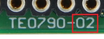
Figure 4: Module hardware revision number.
...
Date | Revision | Contributors | Description | ||||||||
|---|---|---|---|---|---|---|---|---|---|---|---|
| Ali Naseri | initial document |
Table 1415: Document change history.
...
Overview
Content Tools