Page History
...
| HTML |
|---|
<!-- General Notes: Designate all graphics and pictures with a number and a description. For example "Figure 1: TE07xx-xx Block Diagram" or "Table 1: Initial delivery state". "Figure x" and "Table x" have to be formatted to bold. --> |
| scroll-ignore | |
|---|---|
| scroll-pdf-ignore | |
Table of Contents
|
Overview
| Scroll Only (inline) |
|---|
https://wiki.trenz-electronic.de/display/PD/TEI0004+TRM for the current online version of this manual and other available documentation. |
The Trenz Electronic TE0790 is an universal USB2.0 to JTAG, UART and GPIO adapter based on the FTDI FT2232H USB2 IC. The adapter board converts signals from USB2.0 to standard serial or parallel interfaces of Embedded Systems like JTAG, SPI, I²C and UART.
The board is equipped with a programmable System Controller CPLD provided by Lattice Semiconductor LCMXO2-256HC (MachXO2 Product Family) to control the signals of the configured interfaces. The data stream of the USB2.0 port can be also converted to 8 independent GPIO's or used as FIFO.
In order to work with Xilinx tools special order must be used, in that case the EEPROM is pre-programmed and serialized and will be recognized by all Xilinx tools (ISE/Impact/Chipscope, Vivado Programmer/SDK..).
Following table describes the possible operation modes of the TE0790 adapter board. The operation modes are determined by the configuration of the FT2232H (done by programing the Configuration EEPROM) and the firmware implementation of the System Controller CPLD:
...
Arrow USB Programmer2 is an FT2232H based JTAG Adapter supported by Intel Quartus.
Key Features
- Supported by Intel Quartus (JTAG Mode only)
- Intel JTAG Compatible Pinout
- Additional UART Channel available
- Based on FTDI FT2232H USB2 Interface
- Micro USB Connector
- RED activity LED
- GREEN Power-on LED
Table 1: Initial delivery state of programmable devices on the module.
MPSSE - FTDI protocol that is used by JTAG and SPI adapters based on FTDI devices.
Key Features
- Xmod form-factor
- size: 20 x 25 mm
- M3 mounting hole
- FT2232H
- USB2.0 port High Speed (480 Mbps) and Full Speed (12 Mbps) compatible
- Entire USB protocol handled on the chip
- USB2.0 to JTAG, SPI and I²C conversion provided by the IC's Multi-Protocol Synchronous Serial Engine (MPSSE)
- USB2.0 to UART conversion
- Channel B UART RX/TX LED's
- Mini-USB B connector (more rigid then micro-USB)
- 93C56 EEPROM
- Lattice XO2-256 CPLD
- on board programmable using Lattice tools
- 8 universal I/O pins
- VCCIO either 3.3V or user supplied (1.8 to 3.3V)
- RED user LED
- 12 MHz clock from on-board Oscillator
- Variable power supply of the XMOD adapter board
- by Mini USB2.0 connector
- by base-board through pin header J2
- GREEN Power-on LED
- User button
- 4 position DIP switch
- Choose CPLD program mode
- FTDI EEPROM disable (not implemented in PCB REV 1)
- Use VIO same as VCC
- Use VCC from USB
Block Diagram
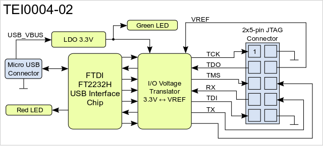
Figure 1: TE0790 TEI0004-02 block diagramBlock Diagram.
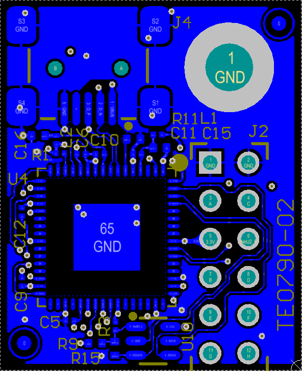
Main Components
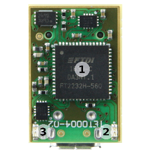
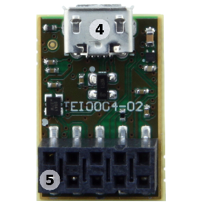
Figure 2: TE0790TEI0004-02 main components.
- FTDI FT2232H IC U4
- 2x6 Pin Header (2.54mm, female), J2
- Mini USB B Connector J4
- Microchip 93AA56BT-I/OT Configuration EEPROM, U10
- DIP-switch S2
- Push button S1
- Lattice Semiconductor LCMXO2-256HC System Controller CPLD, U1
- SiTime SiT8008AI-73 oscillator @12MHz, U6
- Green LED, D1 (Power)
- Red LED, D4 (User)
- Red LED, D3 (UART RX)
- Red LED, D2 (UART TX)
Initial Delivery State
...
Storage device name
...
Content
...
Notes
...
- RED LED (Activity)
- Green LED (Power-on)
- Micro USB2 Connector
- 2x5-pin JTAG Connector (White dot marks Pin 1)
Table 2: Initial delivery state of programmable devices on the module.
Signals, Interfaces and Pins
2x6 Pin Header
JTAG Connector Pinout
The 2x5 female socket The 2x6 pin header (2.54mm grid size, female) J2 have to be connected to the corresponding pin header on the target system. The signal assignment of the pin header on the adapter board depends on the configuration of the System Controller CPLD firmware.
Basic pin assignment:
...
is fully compatible to original USB blaster. Furthermore there is also an UART interface available and I/O-pin reserved for future use.
Following table describes the pin-assignment to the signals of the interfaces:
| Signal | Pin Number | Pin Number | Signal |
|---|---|---|---|
| TCK |
...
Top View
...
Bottom View flipped
...
The signals of the FTDI FT2232H chip are not directly connected to the pin header J2 but routed to the System Controller CPLD of the adapter board, which controls and by-passes the signals to the pin header J2.
Therefore, different signal assignments are made on the pin header J2 depending on the SC CPLD firmware:
Signal assignment on TE0790 CPLD - XMOD Standard:
| (output from adapter) |
| 1 |
| 2 |
| GND |
| TDO (input to adapter) |
| 3 |
...
| 4 |
...
| Reference I/O-voltage from target board for JTAG and UART | |
| TMS ( |
Signal assignment on Standard with RXD-TXD Swapped:
This is the same as the standard configuration except that UART RXD and TXD pins are swapped.
| output from adapter) |
| 5 |
Table 5: Pin header J2 signal assignment with standard, but RXD-TXD swapped configuration firmware. *pin 1 on header J2
Signal assignment on TE0790 CPLD - XMOD DIP40:
On DIPFORTy, VIO Pin is connected with VDD 3.3V Pin. UART RXD is connected to FPGA-Pin L13 and UART TXD to K15. Connect XMOD on the top-side (FPGA side) of the PCB.
| 6 | Reserved Output (May be used as Processor Reset in future software releases) |
| UART RX ( |
| input to adapter) |
| 7 | 8 | UART TX |
| (output from adapter) |
| TDI (output from adapter) |
| 9 |
| 10 | GND |
Table 1: JTAG Connector pin assignmentTable 6: Pin header J2 signal assignment with DIPFORTy firmware.
USB Interface
The USB2.0 USB interface is provided by the FTDI FT2232H chip accessible by the Mini-USB B connector J4IC. The entire USB protocol is handled on chip and compatible to USB2USB 2.0 High Speed (480 MBps) and Full Speed (12 MBps).
On-board Peripherals
FTDI FT2232H IC
The FTDI FT2232H chip provides a variety of industry standard serial or parallel interfaces. On the TE0790 adapter board at current available SC CPLD firmware the functions USB2.0 to JTAG, UART and user GPIO's.
By programing the firmware of the SC CPLD and special EEPROM configurations further further functionalities are available of the FTDI chip which converts signals from USB2.0 to a variety of standard serial and parallel interfaces. Refer to the FTDI data sheet to get information about the capacity of the FT2232H IC.
Configuration EEPROM
The external EEPROM can be used to customize the TE0790 adapter board by setting numerous parameters of the FT2232H IC, enabling different functionalities and configuring serial or parallel interfaces.
The EEPROM is programmable in-circuit over USB using a utility program called FT_PROG available from FTDI’s web site (www.ftdichip.com).
| Warning |
|---|
Important notice on TE0790-xx variants: Do not access the FT2232H EEPROM using FTDI programming tools, doing so will erase normally invisible user EEPROM content and invalidate stored Xilinx JTAG license. Without this license the on-board JTAG will not be accessible any more with any Xilinx tools. Software tools from FTDI website do not warn or ask for confirmation before erasing user EEPROM content. |
System Controller CPLD
The System Controller CPLD (U1) is provided by Lattice Semiconductor LCMXO2-256HC (MachXO2 Product Family). The SC-CPLD is the central system management unit where essential control signals are logically linked by the implemented logic in CPLD firmware, which generates output signals to control the system, the on-board peripherals and the interfaces.
Signals of the serial or parallel interfaces are by-passed, forwarded and controlled by the System Controller CPLD.
The internal routing of the signals on the System Controller CPLD between the USB2.0 interface and pin header J2 depends on its configured firmware. CPLD can be set into JTAG chain via S2-1 DIP Switch. Refer to the TE0790 CPLD Firmware for more information about the currently available System Controller CPLD firmware and for download.
DIP-switch
The DIP-switch S2 is to set different modes of powering the on-board components, the I/O voltages and to enable programming the adapter board CPLD by JTAG interface:
...
The voltages 3.3V (VCC) and VIO (variable SC CPLD I/O-voltage) can be configured by the DIP-switches S2-3 and S2-4:
...
3.3V (pin 5) and VIO (pin 6) sourced USB
IC Channel A is used in MPPSE Mode for JTAG, Channel B is available as UART. FT2232H EEPROM is programmed with Arrow Programmer2 Identificator to be recognized by the support library for Quartus.
On-board LEDs
On-board LEDs indicating power-on and JTAG activity:
| Color | Description |
|---|---|
| Green | Power-on LED |
| Red | JTAG activity |
Table 2
Table 8: DIP-switch S2 power setting description. *Attention: don't supply voltage from base if pin sourced from USB! For more details see Power supply of the adapter board section.
User Push Button
The user push button S1 directly connected to the SC CPLD manipulates pin G of the pin header J2 by driving it to GND.
On-board LEDs
The on-board LEDs indicates system status data transmission activities:
...
Table 9: On-board LEDs.
Power
...
Power supply of the adapter board
The XMOD can be powered via USB or with 3.3V on J2 pins, depending on DIP-switch settings. Max. ~100mA for external components are available on J2 3.3V Pin, if the power supply via USB is used.
Following diagram shows how the settings of the DIP-switches S2-3 and S2-4 determines the configuration of the on-board voltages:

Figure 4: TE0790 on-board voltages configuration
Power Rails
...
Power Rail Name
...
Pin Header J2
...
Direction
...
Arrow Programmer2 is powered via USB.
Table 10: power rails.
Variants Currently In Production
...
Module Variant
...
Xilinx Vivado/SDK Support
...
Table 11: Module variants.
Variants with TE-0790-xxL do not include the ID String in EEPROM for direct support from Xilinx Vivado.
Technical Specifications
Absolute Maximum Ratings
| Parameter | Min | Max | Units | Reference Document |
|---|
VREF | -0. |
| 5 | 4 |
| .6 | V |
| Nexperia 74AVCH4T245 data sheet | |||
| USB VBUS | 4.75 | 5.25 | V |
| USB 2.0 Specification |
| Voltage on I/O pins |
| -0.5 |
| 4. |
| 6 | V |
| Nexperia 74AVCH4T245 data sheet | |
| Storage temperature | -40 |
| +90 | °C |
| LED 19-213/R6C-AL1M2VY/3T data sheet |
Table 123: Module absolute Absolute maximum ratings.
Recommended Operating Conditions
| Parameter | Min | Max | Units | Reference Document |
|---|
VREF |
| 0. |
| 8 | 3.6 | V |
| Nexperia 74AVCH4T245 data sheet |
| USB VBUS | 4.75 | 5.25 | V |
| USB 2.0 Specification |
| Voltage on I/O pins |
| 0 | VREF |
| V |
| Nexperia 74AVCH4T245 data sheet | ||||
| Operating temperature | -40 | +85 | °C | FTDI FT2232H data sheet |
Table 134: Module recommended Recommended operating conditions.
Operating Temperature Range
Industrial grade: -40°C to +85°C.
The TE0790 USB2.0 adapter board is capable to be operated at industrial grade Arrow Programmer2 can be used within industrial temperature range.
Physical Dimensions
Module size: 24,65mm 14.2mm × 20,02mm.8mm. Please download the assembly diagram for exact numbers.
Mating height with standard pin headers: 9.5 mm.
PCB thickness: 1.6 mm.
Highest part on PCB: approx7. 7 37 mm. Please download the step model for exact numbers.
All dimensions are given in millimeters and mil.
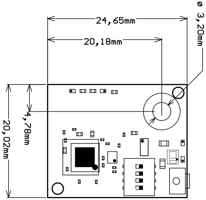
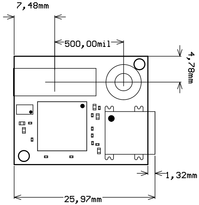
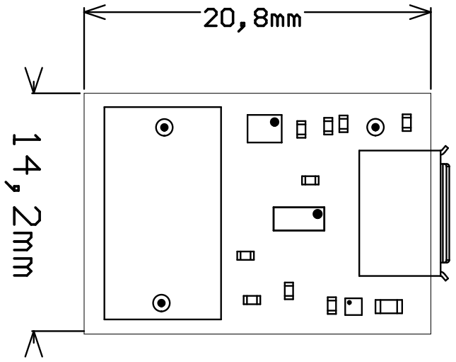
Figure 53: Module physical Physical dimensions drawing.
Revision History
Hardware Revision History
| Date | Revision | Notes | PCN | Documentation Link |
|---|---|---|---|---|
| - | 01 |
| Prototypes | - | - |
| - | 02 |
| First production release. | - |
| TEI0004 |
Table 145: Module hardware Hardware revision history.
Hardware revision number can be found on the PCB board together with the module model number separated by the dash.
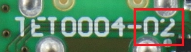
Figure 64: Module hardware revision Revision number.
Document Change History
| HTML |
|---|
<!-- Generate new entry: 1.add new row below first 2.Copy "Page Information Macro(date)" Macro-Preview, Metadata Version number, Author Name and description to the empty row. Important Revision number must be the same as the Wiki document revision number 3.Update Metadata = "Page Information Macro (current-version)" Preview+1 and add Author and change description. --> |
Date | Revision | Contributors | Description |
|---|---|---|---|
|
|
|
- Updated Power supply, DIP-Switch and CPLD section
2017-10-26
v.27- Update 2x6 Pin Header Figure 3
- Update Links
v.26- Initial document
|
|
|
| ||||||||||||||||||||||
2022-05-05 | v.50 | John Hartfiel |
| ||||||||||||||||||||||
| 2017-11-23 | v.31 | Ali Naseri | updated block diagram | ||||||||||||||||||||||
2017-11-21 | v.25 | Ali Naseri |
|
Table 6Table 15: Document change history.
Disclaimer
| Include Page | ||||
|---|---|---|---|---|
|
...
Overview
Content Tools