Page History
...
JTAG Signal | B2B Connector Pin | XMOD Header JB3 | Note |
|---|---|---|---|
| TCK | JB2-119 | JB3-4 | - |
| TDI | JB2-115 | JB3-10 | - |
| TDO | JB2-117 | JB3-8 | - |
| TMS | JB2-113 | JB3-12 | - |
| JTAGSEL | JB2-111 | - | Select SoM's JTAG programming mode on DIP-switch S2-1. |
...
For the same GbE transceiver PHY on the mounted SoM, on the Carrier Board is also a SGMII (Serial Gigabit Media Independent Interface) available. The SGMII pins are available on VG96 connector J9:
| GbE PHY Signal Schematic Name | B2B | Connected to | Notes |
|---|---|---|---|
| SIN_P | JB2-52 | J9-A16 | - |
| SIN_N | JB2-54 | J9-A17 | - |
| SOUT_P | JB2-58 | J9-A19 | - |
| SOUT_N | JB2-60 | J9-A20 | - |
...
When using XMOD FTDI JTAG Adapter TE0790, set the adapter-board's VCC and VCCIO will be sourced by the Carrier Board. Set the DIP-switch with the setting:
- S2-1: ON
- S2-2: OFF
- S2-3: OFF
- S2-4: ON
...
On-board Peripherals
| HTML |
|---|
<!-- Components on the Module, like Flash, PLL, PHY... --> |
...
| DIP-switches S2 | Signal Schematic Net Name | Function | Note |
|---|---|---|---|
| S2-1 | JTAGSEL | Select Zynq chip or SC CPLD programming of mounted SoM: OFF: Zynq chip programming. | Depends also on SoM's SC CPLD firmware configurationRefer also to the TE0729 SC CPLD TRM for detailed information about JTAG update. |
| S2-2 | BOOT_MODE1 | Select first bit of Zynq chip boot mode code | Refer to TE0729 TRM and SC CPLD TRM for detailed information about boot modes. |
| S2-3 | BOOT_MODE2 | Select second bit of Zynq chip boot mode code | - |
| S2-4 | x | x | not used |
...
Following table describes how to configure the VCCIO of the SoM's banks with jumpers:
| VCCIO vs. voltage levelsVoltage Levels | VCCIO_13 | VCCIO_33 | Note |
|---|---|---|---|
| 1.8V | J7:1-2 | J6:1-2 | - |
| 2.5V | J7: 3-4 | J6:3-4 | - |
| 3.3V | J7: 5-6 | J6: 5-6 | - |
...
The Carrier Board's push button S1 is connected to the 'NRST_IN' signal of , the mounted SoM. The function of the button is to trigger a reset of the mounted SoM by driving the reset-signal 'NRST_IN' to ground.
...
| LED | Color | Connected to | Description and Notes |
|---|---|---|---|
| D1 | Red | 'MIO9', pin JB2- 88 | user LED |
Table 15: On-board LEDs.
...
Power Distribution Dependencies
Regulator dependencies and max. current.
Put power distribution diagram here...
The Carrier Board needs one single power supply voltage with a nominal value of 5V. Following diagram shows the distribution of the input voltage '5VIN' to the on-board components on the mounted SoM:
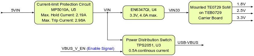
Figure 3: Board Figure : Module power distribution diagram.
See Xilinx data sheet ... for additional information. User should also check related base board documentation when intending base board design for TE07xx module.
Power-On Sequence
The TE07xx SoM meets the recommended criteria to power up the Xilinx Zynq MPSoC properly by keeping a specific sequence of enabling the on-board DC-DC converters dedicated to the particular functional units of the Zynq chip and powering up the on-board voltages.
Following diagram clarifies the sequence of enabling the particular on-board voltages, which will power-up in descending order as listed in the blocks of the diagram:
Put power-on diagram here...
Figure : Module power-on diagram.
Power Rails
Power Rails
| Module Connector (B2B) Module Connector (B2B) Designator | VCC / VCCIO | Direction | Pins | Notes |
|---|---|---|---|---|
| JB1 | VIN33 | Out | Pin 1, 2, 3, 4, 5, 6 | 3.3V module supply voltage |
| VCCIO_13 | Out | Pin 101, 102 | PL IO-bank VCCIO | |
| VCCIO_33 | Out | Pin 29, 30 | PL IO-bank VCCIO | |
| 3.3V | In | Pin 65, 66 | voltage output from module | |
| JB2 | 1.8V | In | Pin 49 | voltage output from module |
| 2.5V | In | Pin 13 | voltage output from module | |
| USB-VBUS | Out | Pin 107 | USB Host supply voltage | |
| VBAT_IN | Out | Pin 118 | RTC buffer voltage |
...
| Main Power Jack and Pins Designator | VCC / VCCIO | Direction | Pins | Notes |
|---|---|---|---|---|
| J12 | 5VIN | In | - | - |
| J9 | 5VIN | In | Pin A1, A2 | '5VIN' power supply to the Carrier Board as alternative to J12 |
| J2 | VBAT_IN | In | Pin 1 | Attention: Pin 2 connected to ground. VBAT_IN voltage on this pin cause short-circuit. |
Table 19: Main Power jack and pins description.
...
| Peripheral Socket Designator | VCC / VCCIO | Direction | Pins | Notes |
|---|---|---|---|---|
| J10 | USB-VBUS | Out | Pin 1 | -USB2.0 Type A socket |
| J11 | USB-VBUS | Out | Pin 1 | -Micro USB2.0 B socket |
| J1 | VIN33 | Out | Pin 4 | MikroSD Card socket VDD |
...
| XMOD Header Designator | VCC / VCCIO | Direction | Pins | Notes |
|---|---|---|---|---|
| JB3 | 3.3V | - | Pin 5 | not connected |
| VIO | In | Pin 6 | connected to VIN33 |
Table 21: Power pin description of XMOD/JTAG Connector.
Board to Board Connectors
...
Variants Currently In Production
NB! Note that here we look at the module as a whole, so you just can't rely only on junction temperature or max voltage of particular SoC or FPGA chip on the module. See examples in the table below.
...
Operating Temperature
...
description of XMOD/JTAG Connector.
Board to Board Connectors
| Include Page | ||||
|---|---|---|---|---|
|
Variants Currently In Production
| Module Variant | Operating Temperature | USB Socket | Temperature Range |
|---|---|---|---|
| TEB0729-02-A | -40°C to +125°C | USB2.0 Type A socket fitted | Industrial |
| TEB0729-02-B | -40°C to +125°C | Micro USB2.0 B socket fitted | Industrial |
Table 22Table : Module variants.
Technical Specifications
Absolute Maximum Ratings
Parameter | Min | Max | Units | Reference Document |
|---|---|---|---|---|
5VIN supply voltage | -0.3 | 7 | V | -MP5010A, EN6347QI data sheet |
Storage temperature | -65 | 150 | °C | - |
Table 23: Module absolute maximum ratings.
...
absolute maximum
...
ratings.
Recommended Operating Conditions
| Parameter | Min | Max | Units | Reference Document |
|---|
| 5VIN supply voltage |
| 4.75 | 5.25 | V | USB2.0 specification concerning 'VBUS' voltage |
| Operating temperature | -40 |
| 125 |
| °C |
| - |
Table 24: Module recommended operating conditions.
Operating Temperature Ranges
...
Extended grade: 0°C to +85°C.
Industrial grade: -40°C to +85°C.
Module operating temperature range depends also on customer design and cooling solution. Please contact us for optionsThe TEB0729 Carrier Board is capable to be operated at industrial grade temperature range.
Physical Dimensions
Board size: 107.70 mm × 100 mm. Please download the assembly diagram for exact numbers.
Mating height with standard connectors: ... 8 mm.
PCB thickness: ca. 1.65mm. mm.
Highest part on PCB: approx. ... mmthe PCB is the Ethernet RJ-45 jack, which has an approximately 17 mm overall height. Please download the step model for exact numbers.
All dimensions are given in millimeters.
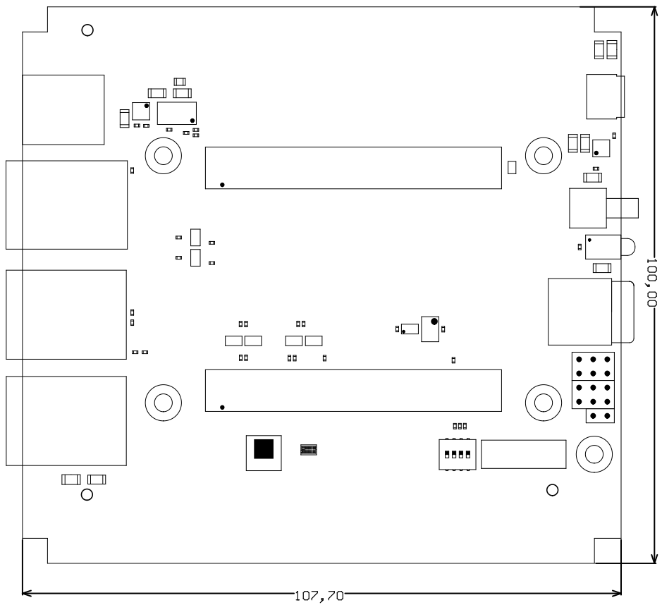
Figure 4: Board physical dimensions drawing.
...
| Date | Revision | Notes | PCN | Documentation Link | |
|---|---|---|---|---|---|
| - | 01 | Prototypes | - | - | |
| - | 02 | First Production Release | - | TEB0729-02 |
Table 25: Module hardware revision history.
Hardware revision number can be found on the PCB board together with the module model number separated by the dash.
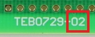 Put picture of actual PCB showing model and hardware revision number here...
Figure 5: Module hardware revision number.
...
Date | Revision | Contributors | Description | ||||||||
|---|---|---|---|---|---|---|---|---|---|---|---|
| Ali Naseri | initial document |
Table 26: Document change history.
...
Overview
Content Tools