Page History
...
| HTML |
|---|
<!-- Download Link: Go to Base Folder of the Module or Carrier, for example : https://shop.trenz-electronic.de/en/Download/?path=Trenz_Electronic/TE0712 Use english URL "../en/.. --> |
| Scroll Ignore |
|---|
| Scroll pdf ignore | |
|---|---|
Table of Contents
|
...
| Scroll Only (inline) |
|---|
Refer to https://wiki.trenz-electronic.de/display/PD/TE0706TEBA0841+TRM for the current online version of this manual and other available documentation. |
The Trenz Electronic TE0706 TEBA0841 is a Carrier Board provides functionalities for testing, evaluation and development purposes of company's 4 x 5 cm SoMs. The Carrier Board is equipped with various components and connectors for different configuration setups and needs. The interfaces of the SoM's functional units and PL I/O-banks are connected via board-to-board connectors to the Carrier Board's components and connectors for easy user access., especially for the Multi-gigabit transceiver units of the TE0841 and TE0741 modules. Although this base-board is dedicated to the modules TE0841 and TE0741, it is also compatible with other Trenz Electronic 4 x 5 cm SoMs.
See page See "4 x 5 cm carriers" page for more to get information about supported 4 x 5 cm SoMsthe SoMs supported by the TEBA0841 base-board.
Key Features
- SFP+ connector (Enhanced small form-factor pluggable), supports data transmission rates up to 10 Gbit/s
- Micro USB2.0 Type B Connector (J10)
- Trenz 4x5 module Socket (3 x Samtec LSHM series connectors)
- 4 x 5 SoM programmable by XMOD JTAG/UART header (JX1)
- 2 x user LEDs routed to I/O-pins of the SoM
- Soldering-pads J17 and J20 for optional pin headers for access to SoM's I/O-bank-pins, usable as LVDS-pairs
- Soldering-pads J3 and J4 for optional pin headers for access to further interfaces and I/O's of the SoM
- 3 x Samtec LSHM Series Board to Board Connectors
- VG96 connector (mounting holes and solder pads, J6) and 50-pin IDC male connector socket (J5) for access to PL I/O-bank pins
- Micro SD card socket
- SDIO port expander with voltage-level translation
- USB2.0 type A connector, optionally Micro USB 2.0 connector
- 1 x user-push button S2, by default configured as system reset button
- 1 x RJ45 GbE MagJack J3, connected via MDI to B2B connector JB1
- 1 x Marvell Alaska 88E1512 GbE PHY, providing Ethernet interface in conjunction with RJ45 GbE MagJack J2
- 5V power supply barrel jack
- 4 A High-Efficiency Power SoC DC-DC Step-Down Converter (Enpirion EN6347) for 3.3V power supply
- XMOD JTAG- / UART-header JX1
- DIP-switch S1 to set Som's System Controller CPLD control signals
- 3 x VCCIO selection jumper J10, J11 and J12 to set SoM's PL I/O-bank voltages
Additional assembly options are available for cost or performance optimization upon request.
Block Diagram
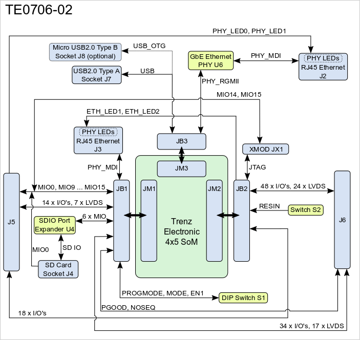
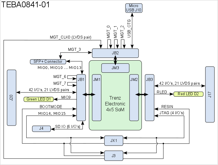
Figure 1: TE0706-02 block diagram TEBA0841-01 Block Diagram.
Main Components
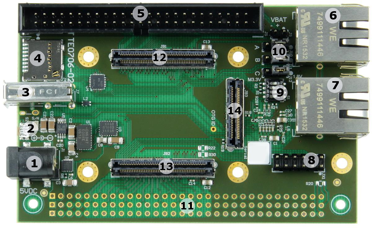
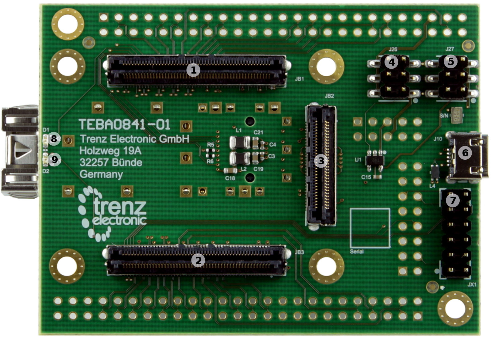
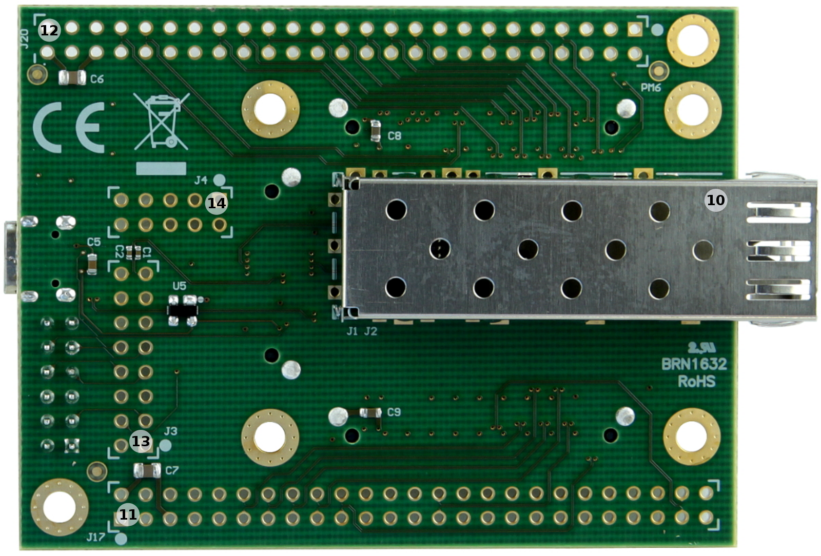
Figure 2: TE0706-02 Carrier Board
- Samtec Razor Beam™ LSHM-150 B2B connector, JB1
- Samtec Razor Beam™ LSHM-150 B2B connector, JB3
- Samtec Razor Beam™ LSHM-130 B2B connector, JB2
- 6-pin header J26, for selecting PL I/O-bank voltage
- 6-pin header J27, for selecting PL I/O-bank voltage
- Micro USB2.0 Type B Connector J12 (Device or OTG mode)
- JTAG/UART header, JX1 ('XMOD FTDI JTAG Adapter'-compatible pin-assignment)
- User LED D1 (green)
- User LED D2 (red)
- SFP+ Connector, J1
- 50-pin header soldering-pads J17, for access to PL I/O-bank pins (LVDS-pairs possible)
- 50-pin header soldering-pads J20, for access to PL I/O-bank pins (LVDS-pairs possible)
- 16-pin header soldering-pads J3, JTAG/UART header ('XMOD FTDI JTAG Adapter'-compatible pin-assignment)
- 10-pin header soldering-pads J4, for access to SoM's SDIO-port, if available
- 5V power connector jack, J1
- Reset switch, S2
- USB2.0 type A receptacle, J7
- Micro SD card socket with Card Detect, J4
- 50 pin IDC male connector, J5
- 1000Base-T Gigabit RJ45 Ethernet MagJack, J3
- 1000Base-T Gigabit RJ45 Ethernet MagJack, J2
- XMOD JTAG- / UART-header, JX1
- User DIP-switch, S1
- VCCIO selection jumper block, J10 - J12
- External connector (VG96) placeholder, J6
- Samtec Razor Beam™ LSHM-150 B2B connector, JB1
- Samtec Razor Beam™ LSHM-150 B2B connector, JB2
- Samtec Razor Beam™ LSHM-130 B2B connector, JB3
Initial Delivery State
Board is shipped in following configuration:
- VCCIO voltage selection jumpers are all set to 1.8 V.
- S2 switch configured as reset button.
- One VG96 connector Pin headers (not soldered to the board, but included in the package as separate component)
...
| HTML |
|---|
<!-- Connections and Interfaces or B2B Pin's which are accessible by User --> |
B2B Connector
With the TE0706 TEBA0841 Carrier Board's Board-to-Board Connectors (B2B) the MIO- and PL I/O-bank's pins and further interfaces of the mounted SoM can be accessed. A large quantity of these I/O's are also usable as LVDS-pairs. The connectors provide also VCCIO voltages to operate the I/O's properly.
...
Table 12: DIP-switch S1 SoM configuration settings.
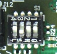
Figure 3: User DIP-switch S1
...
Table 13: VCCIO jumper settings.
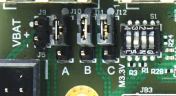
Figure 4: Base-board supply-voltages (VCCIOA, VCCIOB, VCCIOC) selection jumpers.
...
The Carrier Board needs one single power supply voltage with a nominal value of 5V. Following diagram shows the distribution of the input voltage '5VIN' to the on-board components on the mounted SoM:
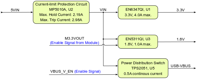
Figure 5: Board power distribution diagram.
...
All dimensions are given in millimeters.
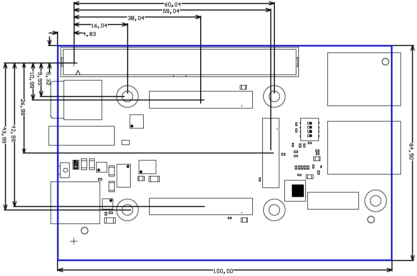
Figure 6: Board physical dimensions drawing.
...
Hardware revision number can be found on the PCB board together with the module model number separated by the dash.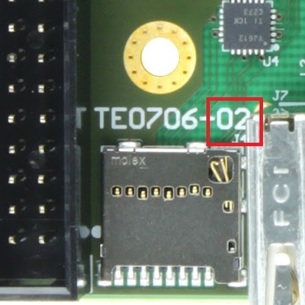
Figure 7: Board hardware revision number.
...
Overview
Content Tools