Page History
...
Figure 1: TEBA0841-01 Block Diagram.
Main Components
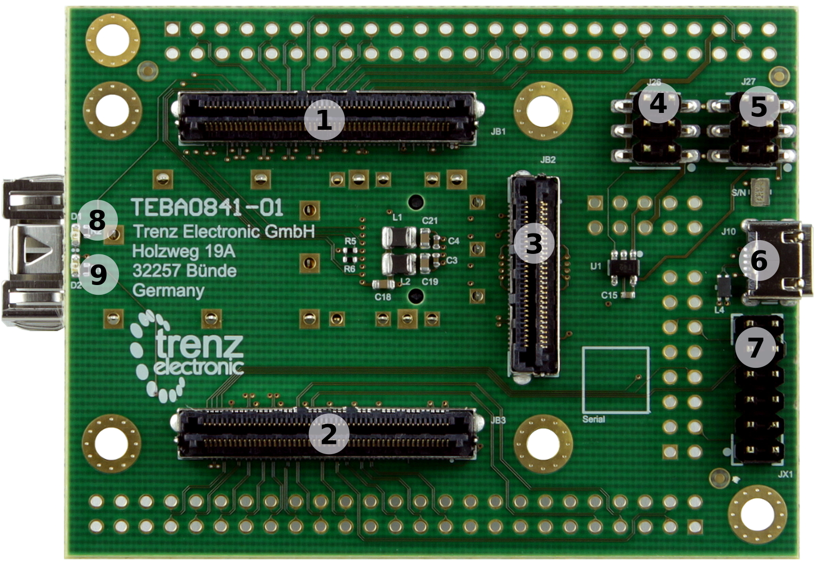
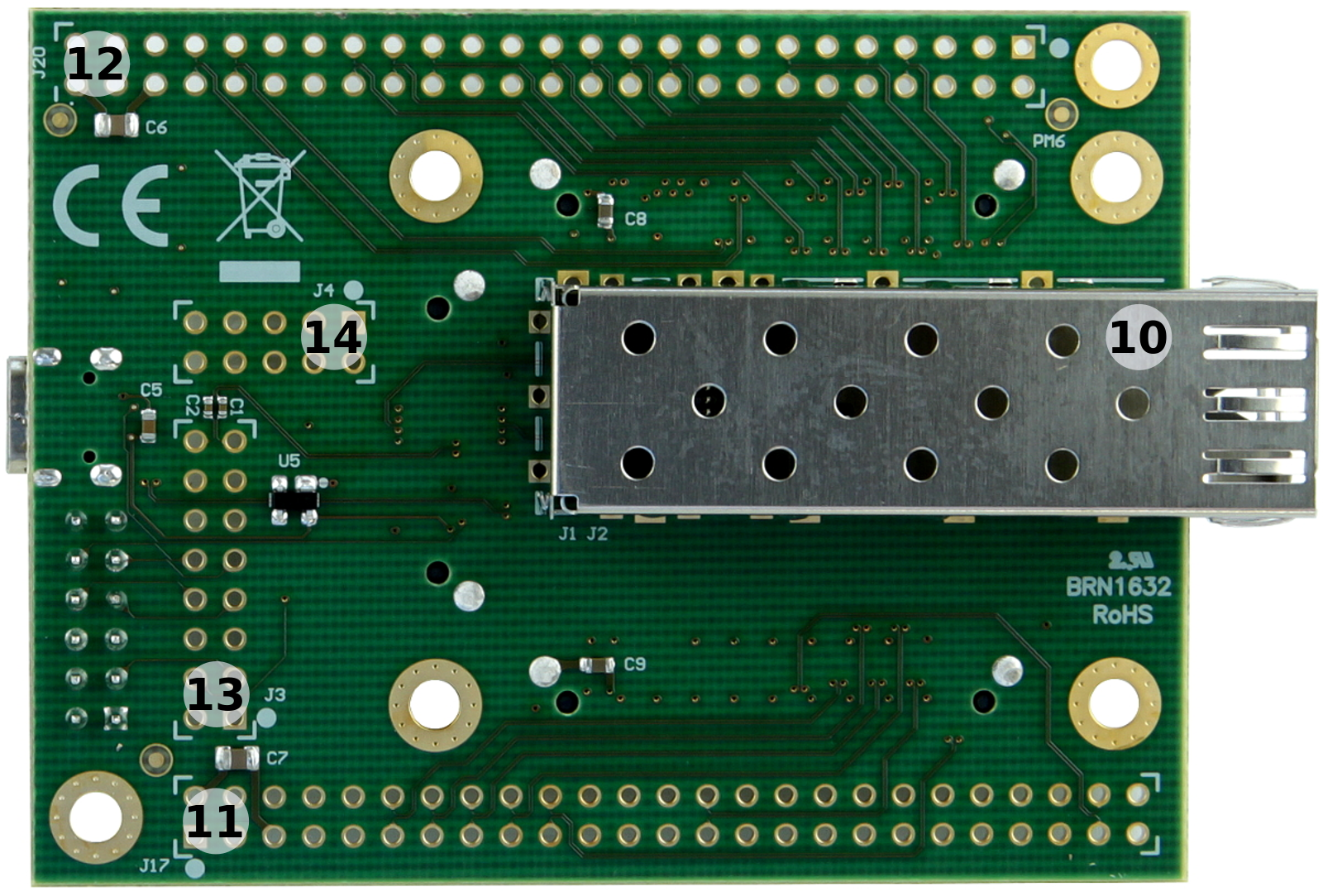
Figure 2: TEBA0841-01 Carrier Board.
...
Following table gives a summary of the available I/O's, interfaces and differential pairs of the B2B connectors JB1, JB2 and JB3:
| B2B Connector | Interfaces | Count of I/O's | Notes |
|---|---|---|---|
| JB1 | User I/O | 42 single ended or 21 differential | - |
| SD IO | 6 | - | |
| MIO | 8 | - | |
| SoM control signals | 1 | 'BOOTMODE' | |
| JB2 | MGT lanes | 8 differential pairs, 4 lanes | - |
| MGT reference input clock | 1 differential pair | ||
| USB2.0 (OTG and device mode) | 4 | - | |
| JB2 | User I/O | 42 single ended 21 differential | -- |
| JTAG | 4 | - | |
| Red user LED | 1 | - | |
| SoM control signals | 1 | 'RESIN' |
Table 1: General overview of PL I/O signals and SoM's interfaces connected to the B2B connectors.
...
Following table gives a summary of the pin-assignment, available interfaces and functional I/O's of the pin headers:
| On-board Pin Header | Control Signals and Interfaces | Count of I/O's | Notes |
|---|---|---|---|
| J17 | User I/O | 42 single ended or 21 differential | - |
| J20 | User I/O | 42 single ended or 21 differential | - |
| J3 | JTAG | 4 | - |
| SoM control signals | 2 | 'RESIN', 'BOOTMODE' | |
| MGT reference input clock | 1 differential pair | AC decoupled on-board (100 nF capacitor) | |
| MIO | 2 | user IO (configurable as UART for example) | |
| J4 | SD IO | 6 | 3.3V and 1.8V voltage level available on header |
Table 2: General overview of PL I/O signals, SoM's interfaces and control signals connected to the on-board connectors.
...
The pin-assignment of the SFP connector is in detail as fellows:
| SFP+ pin | Pin Schematic Name | B2B | FPGA Direction | Description | Note |
|---|---|---|---|---|---|
| Transmit Data + (pin 18) | MGT_TX3_P | JB2-26 | Output | SFP+ transmit data differential pair | - |
| Transmit Data - (pin 19) | MGT_TX3_N | JB2-28 | Output | - | |
| Receive Data + (pin 13) | MGT_RX3_P | JB2-25 | Input | SFP+ receive data differential pair | - |
| Receive Data - (pin 12) | MGT_RX3_N | JB2-27 | Input | - | |
| Receive Fault (pin 2) | MIO10 | JB1-96 | Input | Fault / Normal Operation | High active logic |
| Receive disable (pin 3) 1) | SFP0_TX_DIS | not connected | Output | SFP Enabled / Disabled | Low active logic |
| MOD-DEF2 (pin 4) | MIO13 | JB1-98 | Input | Module present / not present | Low active logic |
| MOD-DEF1 (pin 5) | MIO12 | JB1-100 | Output | 2-wire Serial Interface clock | 3.3V pull-up on-board |
| MOD-DEF0 (pin 6) | MIO11 | JB1-94 | BiDir | 2-wire Serial Interface data | 3.3V pull-up on-board |
| RS0 (pin 7) | SFP0_RS0 | not connected | Output | Full RX bandwidth | Low active logic |
| LOS (pin 8) | MIO0 | JB1-88 | Input | Loss of receiver signal | High active logic |
| RS1 (pin 9) | SFP0_RS1 | not connected | Output | Reduced RX bandwidth | Low active logic |
Table 3: SFP+ connector pin-assignment.
...
The MGT lane pins are bridged on-board as fellows, if 4 x 5 SoM TE0741 is mounted on carrier board:
| MGT Lane | B2B TX Differential Pair | B2B RX Differential Pair | B2B Pins Bridged |
|---|---|---|---|
| MGT-lane 0 | JB2-8 (MGT_TX0_N) JB2-10 (MGT_TX0_P) | JB2-7 (MGT_RX0_N) JB2-9 (MGT_RX0_P) | JB2-7 to JB2-8 JB2-9 to JB2-10 |
| MGT-lane 1 | JB2-14 (MGT_TX1_N) JB2-16 (MGT_TX1_P) | JB2-13 (MGT_RX1_N) JB2-15 (MGT_RX1_P) | JB2-13 to JB2-14 JB2-15 to JB2-16 |
| MGT-lane 2 | JB2-20 (MGT_TX2_N) JB2-22 (MGT_TX2_P) | JB2-19 (MGT_RX2_N) JB2-21 (MGT_RX2_P) | JB2-19 to JB2-20 JB2-21 to JB2-22 |
| MGT-lane 7 | JB1-3 (MGT_TX7_P) JB1-5 (MGT_TX7_N) | JB1-9 (MGT_RX7_P) JB1-11 (MGT_RX7_N) | JB1-3 to JB1-9 JB1-5 to JB1-11 |
| MGT-lane 6 | JB1-15 (MGT_TX6_P) JB1-17 (MGT_TX6_N) | JB1-21 (MGT_RX6_P) JB1-23 (MGT_RX6_N) | JB1-15 to JB1-21 JB1-17 to JB1-23 |
Table 4: Looped-backed MGT-lanes for mounted 4 x 5 SoM TE0741.
...
JTAG access to the mounted SoM is provided through B2B connector JB2 and is also routed to the XMOD header JX1 and pin header J3. With the TE0790 XMOD USB2.0 to JTAG adapter, the device of the mounted SoM can be programed via USB2.0 interface.
JTAG Signal | B2B Connector Pin | XMOD Header JX1 | Pin Header J3 | Note |
|---|---|---|---|---|
| TCK | JB3-100 | JX1-4 | J3-4 | - |
| TDI | JB3-96 | JX1-10 | J3-10 | - |
| TDO | JB3-98 | JX1-8 | J3-8 | - |
| TMS | JB3-94 | JX1-12 | J3-12 | - |
Table 5: JTAG interface signals.
...
UART interface is available on B2B connector JB1 and is usually established by MIO-pins of the PS-bank of the mounted SoM's Zynq device. With the TE0790 XMOD USB2.0 adapter, the UART signals can be converted to USB2.0 interface signals:
| UART Signal Schematic Name | B2B | XMOD Header JX1 | Pin Header J3 | Note |
|---|---|---|---|---|
| MIO14 | JB1-91 | JX1-7 | J3-7 | UART-RX (receive line) |
| MIO15 | JB1-86 | JX1-3 | J3-3 | UART-TX (transmit line) |
Table 6: UART interface signals.
...
The SD IO interface of the mounted SoM is routed to the pin header J4. Due to the different operation voltage levels of the MicroSD Card socket (3.3V) and the and the SoM's Zynq device MIO-bank (1.8V), a VDD/VCCIO translation is necessary which can be provided for example by Texas Instruments TXS02612 SDIO port expander IC. Both voltage levels are available on pin header J4:
| SD IO Signal Schematic Name | B2B | Pin Header J4 | Note |
|---|---|---|---|
| SD_DAT0 | JB1-24 | J4-8 | SD IO data |
| SD_DAT1 | JB1-22 | J4-10 | SD IO data |
| SD_DAT2 | JB1-20 | J4-9 | SD IO data |
| SD_DAT3 | JB1-18 | J4-7 | SD IO data |
| SD_CLK | JB1-28 | J4-4 | SD IO clock |
| SD_CMD | JB1-26 | J4-3 | SD IO command |
Table 7: SD IO interface signals.
...
Following table gives an overview of the USB2.0 interface signals:
| USB2.0 Signal Schematic Name | B2B | Connected to | Note |
|---|---|---|---|
| OTG_N | JB2-48 | J10-2 | USB2.0 data |
| OTG_P | JB2-50 | J10-3 | USB2.0 data |
| OTG-ID | JB2-52 | J10-4 | Ground this pin for A-Device (host), left floating this pin for B-Device (peripheral). |
| USB-VBUS | JB2-56 | J10-1 | USB supply voltage for Host mode. Not supplied by the Carrier Board. |
Table 8: USB2.0 interface signals and connections.
...
Following table describes the signals and interfaces of the XMOD header JX1 and pin header J3:
| Pin Schematic Name | XMOD Header JX1 Pin | Header J3 Pin | B2B | Note |
|---|---|---|---|---|
| TCK | C (pin 4) | 4 | JB3-100 | - |
| TDO | D (pin 8) | 8 | JB3-98 | - |
| TDI | F (pin 10) | 10 | JB3-96 | - |
| TMS | H (pin 12) | 12 | JB3-94 | - |
| MIO15 | A (pin 3) | 3 | JB1-86 | UART-TX (transmit line) |
| MIO14 | B (pin 7) | 7 | JB1-91 | UART-RX (receive line) |
| BOOTMODE | E (pin 9) | 9 | JB1-90 | usually 'JTAGSEL' on TE 4 x 5 SoMs |
| RESIN | G (pin 11) | 11 | JB3-17 | SoM Reset pin |
| CLK0_N | - | 15 | JB2-32 | AC decoupled on-board (100 nF capacitor) |
| CLK0_P | - | 16 | JB2-34 | AC decoupled on-board (100 nF capacitor) |
Table 9: JTAG/UART header signals and connections.
When using XMOD FTDI JTAG Adapter TE0790, the adapter-board's VCC and VCCIO will be sourced by the on-boards 3.3V supply voltage. Set the DIP-switch with the setting:
| XMOD DIP-switches | Position |
|---|---|
| Switch 1 | ON |
| Switch 2 | OFF |
| Switch 3 | OFF |
| Switch 4 | OFF |
Table 10: XMOD adapter board DIP-switch positions for voltage configuration.
...
The on-board LEDs are available to the user and can be used to indicate system status and activities:
| LED | Color | Pin Schematic Name | B2B Connector | Description and Notes |
|---|---|---|---|---|
| D1 | Green | MIO9 | JB1-92 | available to user |
| D2 | Red | RLED | JB3-90 | available to user |
Figure 11: On-board LEDs
VCCIO Selection Jumper
...
TE 4 x 5 Modules have a standard assignment of PL-bank I/O voltages on their B2B connectors, which will be fed with I/O voltage from base-board.
Base-board PL-bank I/O Voltages | B2B Pins | Standard Assignment of PL-bank I/O Voltages on TE 4x5 Modules |
|---|---|---|
| VCCIOA | JB1-10, JB1-12 | VCCIOA (JM1-9, JM1-11) |
| VCCIOD | JB2-8, JB2-10 | VCCIOD (JM2-7, JM2-9) |
Table 12: Base-board PL-bank I/O voltages VCCIOA and VCCIOD
...
Following table describes how to configure the base-board supply-voltages by jumpers:
Base-board PL-bank I/O Voltages | VCCIOA | VCCIOD |
|---|---|---|
| 1.8V | J26:1-2 | J27:1-2 |
| 2.5V | J26:3-4 | J27:3-4 |
| 3.3V | J26:5-6 | J27:5-6 |
Table 13: Configuration of base-board supply-voltages via jumpers. Jumper-Notification: 'Jx: 1-2' means pins 1 and 2 are connected, 'Jx: 3-4' means pins 3 and 4 are connected, and so on.
...
Xilinx provide a power estimator excel sheets to calculate power consumption. It's also possible to evaluate the power consumption of the developed design with Vivado. See also Trenz Electronic Wiki FAQ.
| Power Input | Typical Current |
|---|---|
| 3.3V | TBD* |
Table 14: Typical power consumption.
...
The external power-supply can be connected to the board by the following pins:
| Connector | 3.3V pin | GND pin |
|---|---|---|
| JX1 | JX1-5, JX1-6, | JX1-1, JX1-2 |
| J3 | J3-5, J3-6 | J3-1, J3-2 |
| J4 | J4-5 | J4-1, J4-2 |
| J20 | J20-5, J20-46 | J20-1 , J20-2 , J20-49 , J20-50 |
| J17 | J17-5, J17-46 | J17-1 , J17-2 , J17-49 , J17-50 |
Table 15: Connector pins capable for external 3.3V power supply
...
The voltage direction of the power rails is from board and on-board connectors' view:
| Module Connector (B2B) Designator | VCC / VCCIO | Direction | Pins | Notes |
|---|---|---|---|---|
| JB1 | 3.3V | Out | 2, 4, 6, 14, 16 | 3.3V module supply voltage |
| VCCIOA | Out | 10, 12 | PL IO-bank VCCIO | |
| M1.8VOUT | In | 40 | 1.8V module output voltage | |
| JB2 | 3.3V_OUT | In | 9, 11 | 3.3V module output voltage |
| 3.3V | Out | 1, 3, 5, 7 | 3.3V module supply voltage | |
| VCCIOD | Out | 8, 10 | PL IO-bank VCCIO | |
| JB3 | USB-VBUS | Out | 56 | USB Host supply voltage |
Table 16: Power pin description of B2B module connector.
| On-board Pin Header Designator | VCC / VCCIO | Direction | Pins | Notes |
|---|---|---|---|---|
| J17 | 3.3V | In / Out | 5, 48 | 3.3V external supply voltage |
| VCCIOD | In / Out | 6, 45 | PL IO-bank VCCIO, depends on Jumper settings | |
| J20 | 3.3V | In / Out | 5, 48 | 3.3V external supply voltage |
| VCCIOA | In / Out | 6, 45 | PL IO-bank VCCIO, depends on Jumper settings |
Table 17: Power Pin description of on-board connector.
| Jumper / Header Designator | VCC / VCCIO | Direction | Pins | Notes |
|---|---|---|---|---|
| J26 | VCCIOA | In | 2, 4, 6 | - |
| M1.8VOUT | Out | 1 | - | |
| 2.5V | Out | 3 | - | |
| 3.3V_OUT | Out | 5 | - | |
| J27 | VCCIOD | In | 2, 4, 6 | - |
| M1.8VOUT | Out | 1 | - | |
| 2.5V | Out | 3 | - | |
| 3.3V_OUT | Out | 5 | - | |
| J4 | 3.3V | Out | 5 | - |
| M1.8VOUT | Out | 6 | - |
Table 18: Power Pin description of VCCIO selection jumper pin header.
| Peripheral Socket Designator | VCC / VCCIO | Direction | Pins | Notes |
|---|---|---|---|---|
| J10 | USB-VBUS | In | 1 | USB Host supply voltage |
Table 19: Power pin description of peripheral connector.
| XMOD Header Designator | VCC / VCCIO | Direction | Pins | Notes |
|---|---|---|---|---|
| JX1 | 3.3V | Out | 5 | connected to 3.3V external supply voltage |
| VIO | Out | 6 | ||
| J3 | 3.3V | Out | 5 | connected to 3.3V external supply voltage |
| 3.3V | Out | 6 |
Table 20: Power pin description of XMOD/JTAG Connector.
...
Technical Specifications
Absolute Maximum Ratings
| Parameter | Min | Max | Units | Notes |
|---|---|---|---|---|
Vin supply voltage | 3.135 | 3.465 | V | 3.3V supply-voltage ± 5% |
Storage Temperature | -55 | 105 | °C | Molex 74441-0001 Product Specification |
Table 21: Board absolute maximum ratings.
Recommended Operating Conditions
| Parameter | Min | Max | Units | Notes |
|---|---|---|---|---|
| Vin supply voltage | 3.135 | 3.465 | V | - |
| Operating temperature | -40 | +85 | °C | Molex 74441-0001 Product Specification |
Table 22: Module recommended operating conditions.
...
Hardware Revision History
| Date | Revision | Notes | PCN | Documentation Link |
|---|---|---|---|---|
| - | 01 |
| - | TEBA0841-01 |
Table 23: Module hardware revision history.
...
| HTML |
|---|
<!-- Generate new entry: 1.add new row below first 2.Copy "Page Information Macro(date)" Macro-Preview, Metadata Version number, Author Name and description to the empty row. Important Revision number must be the same as the Wiki document revision number 3.Update Metadata = "Page Information Macro (current-version)" Preview+1 and add Author and change description. --> |
Date | Revision | Contributors | Description | ||||||||
|---|---|---|---|---|---|---|---|---|---|---|---|
| Ali Naseri, Jan Kumann |
|
Table 24: Document change history.
...
Overview
Content Tools