Page History
...
| HTML |
|---|
<!-- Download Link: Go to Base Folder of the Module or Carrier, for example : https://shop.trenz-electronic.de/en/Download/?path=Trenz_Electronic/TE0712 Use english URL "../en/.. --> |
| Scroll Ignore |
|---|
| Scroll pdf ignore | |
|---|---|
Table of Contents
|
...
| Scroll Only (inline) |
|---|
Refer to https://wiki.trenz-electronic.de/display/PD/TEBA0841TEBB0714+TRM for the current online version of this manual and other available documentation. |
The Trenz Electronic TEBA0841 TEBB0714 is a Carrier Board for testing, evaluation and development purposes, especially for the Multi -gigabit transceiver Gigabit Transceiver units of the TE0841 and TE0741 modulesTE0714 module. Although this base-board is dedicated to the modules TE0841 and TE0741TE0714 module, it is also compatible with other Trenz Electronic 4 x 5 3 cm SoMs. See page "4 x 5 3 cm carriers" to get information about the SoMs supported by the TEBA0841 TEBB0714 Carrier Board.
This base-board provides also solder pads as place-holders for pin headers as option to get access to the PL I/O-bank pins and further of the mounted TE 4 x 3 SoM.
Key Features
- SFP+ connector (Enhanced small form-factor pluggable), supports support data transmission rates up to 10 Gbit/s
- Micro USB2.0 Type B Connector (J10)
- Trenz 4x5 module Socket (3 x Samtec LSHM series connectors)
- 4 Hirose Ultra small SMT coaxial connectors, support data transmission rates up to 6 Gbit/s
- TE 4 x 3 cm 4 x 5 SoM programmable by XMOD JTAG/UART header (JX1)
- 2 x user LEDs routed to I/O-pins of the SoM
- Soldering-Solder pads J17 and J20 for optional pin headers for access to SoM's PL I/O-bank - pins, usable as LVDS - pairs
- Soldering-Solder pads J3 and J4 for optional pin headers for access to further interfaces and I/O's of the SoM
Additional assembly options are available for cost or performance optimization upon request.
Block Diagram
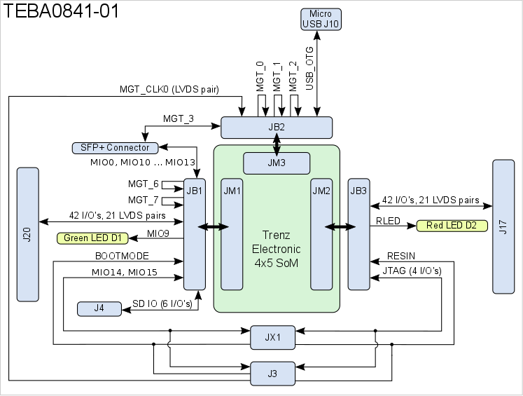
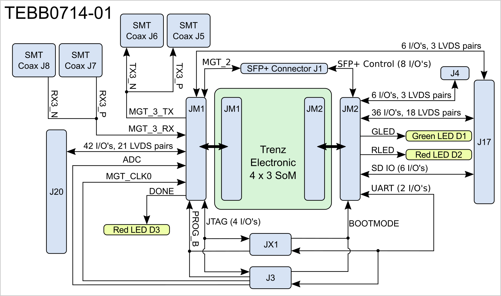
Figure 1: TEBA0841TEBB0714-01 Block Diagram.
Main Components
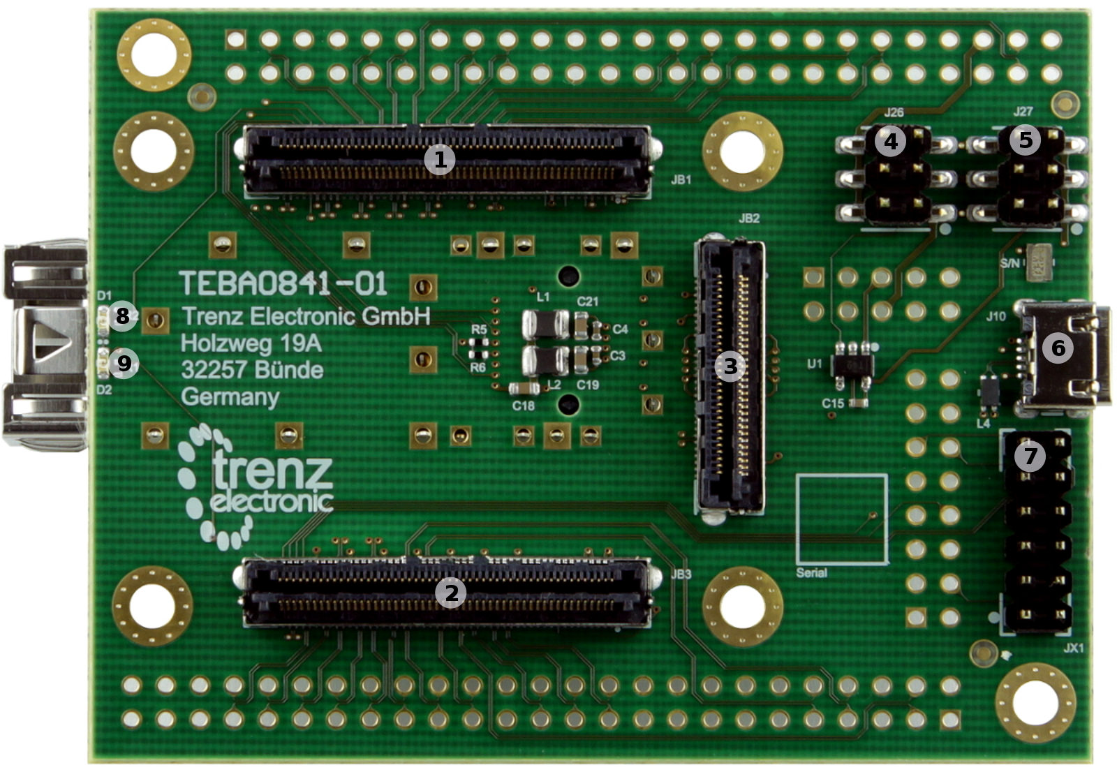
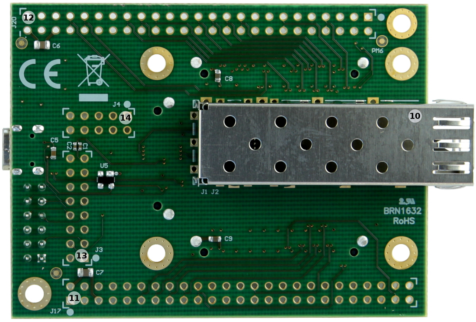
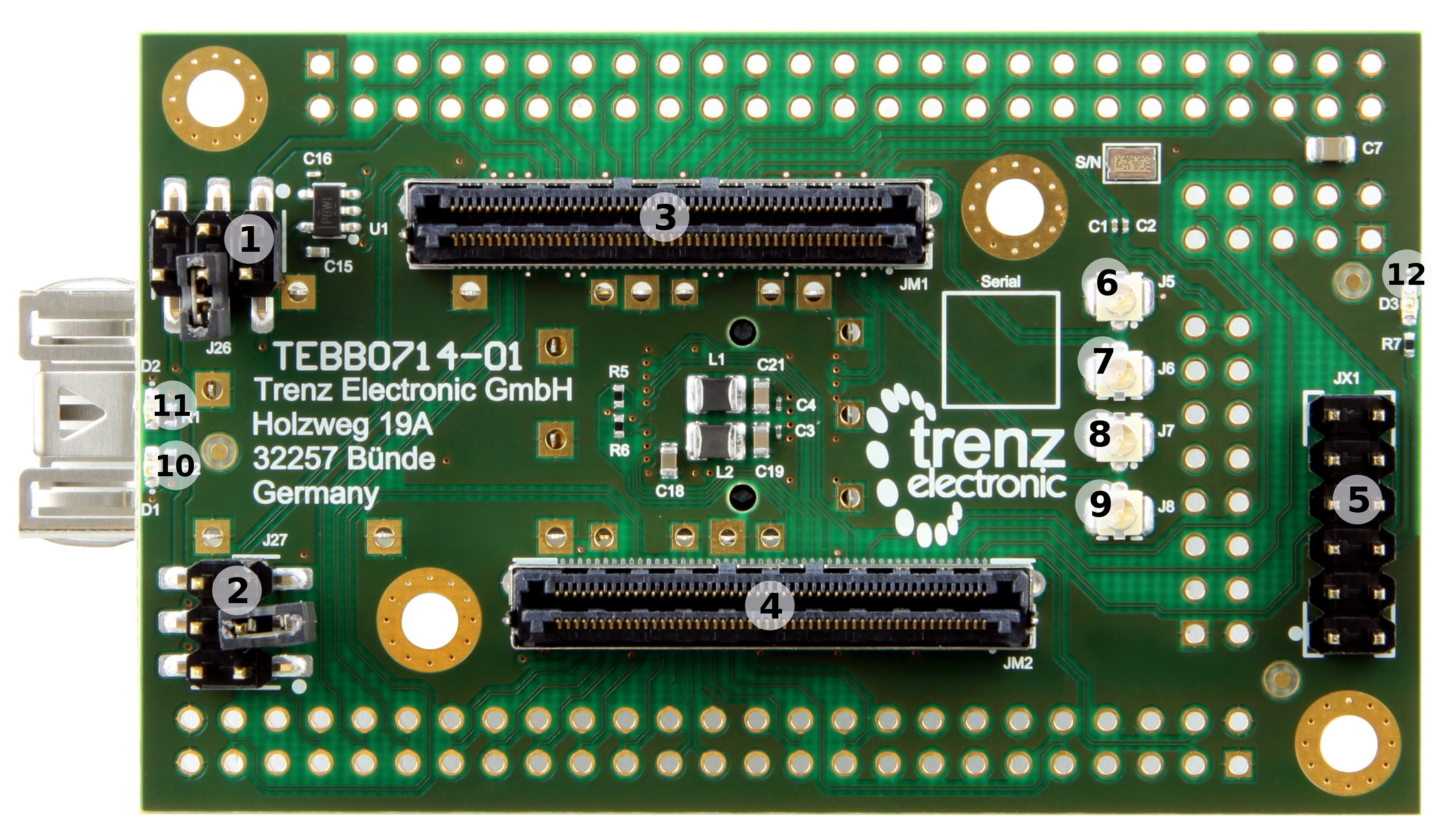
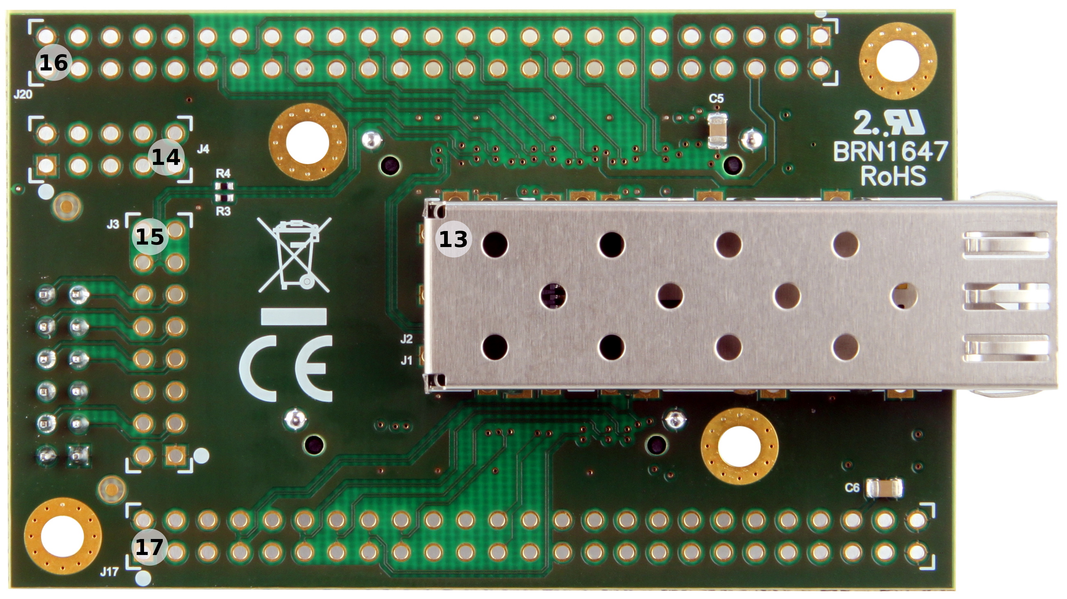
Figure 2: TEBA0841TEBB0714-01 Carrier Board.
- 6-pin header J26 for selecting PL-bank I/O voltage
- 6-pin header J27 for selecting XMOD/JTAG VCCIO
- Samtec Razor Beam™
- Samtec Razor Beam™ LSHM-150 B2B connector, JB1
- Samtec Razor Beam™ LSHM-150 B2B connector, JB3JM1
- Samtec Razor Beam™ LSHM-130 B2B 150 B2B connector, JB2JM2
- 6-pin header J26, for selecting PL I/O-bank voltage
- 6-pin header J27, for selecting PL I/O-bank voltage
- Micro USB2.0 Type B Connector J12 (Device or OTG mode)
- XMOD header, JX1
- Ultra small SMT coaxial connector, J5
- Ultra small SMT coaxial connector, J6
- Ultra small SMT coaxial connector, J7
- Ultra small SMT coaxial connector, J8JTAG/UART header, JX1 ('XMOD FTDI JTAG Adapter'-compatible pin-assignment)
- User LED D1 (green)
- User LED D2 (red)
- SFP+ Connector, J1
- 50-pin header soldering-pads J17, for access to PL I/O-bank pins (LVDS-pairs possible)
- LED D3 (red) indicating FPGA's 'Programming DONE'-signal
- SFP+ Connector, J1
- 10-pin header solder pads J4 for access to SoM's 50-pin header soldering-pads J20, for access to PL I/O-bank pins banks (LVDS-pairs possible)
- 16-pin header soldering-solder pads J3, JTAG/UART header ('XMOD FTDI JTAG Adapter'-compatible pin-assignment)
- 1050-pin header soldering-pads J4, solder pads J20 for access to SoM's PL I/O-banks (LVDS pairs possible)
- 50-pin header solder pads J17 for access to SoM's SDIO-port, if availablePL I/O-banks (LVDS pairs possible)
Initial Delivery State
Board is shipped in following configuration:
...
| B2B Connector | Interfaces | Count of I/O's | Notes |
|---|---|---|---|
| JB1JM1 | User I/O | 42 single ended or 21 differential | - |
| SD IO | 6 | - | |
| MIO | 8 | - | |
| SoM control signals | 1 | 'BOOTMODE' | |
| JB2 | MGT lanes | 8 differential pairs, 4 lanes | - |
| MGT reference input clock | 1 differential pair | ||
| USB2.0 (OTG and device mode) | 4 | - | JB2|
| User I/O | 42 single ended 21 differential | -- | |
| JTAG | 4 | - | |
| Red user LED | 1 | - | |
| SoM control signals | 1 | 'RESIN' |
...
Overview
Content Tools