Page History
...
| B2B Connector | Interfaces | Count of I/O's | Notes | |
|---|---|---|---|---|
| JM1 | User I/O | 54 single ended or 27 differential | - | |
| MGT lanes | 4 differential pairs, 2 lanes | - | ||
| MGT reference clock input | 1 | - | ||
| JTAG | 4 | - | ||
| SoM control signals | 2 | 'PROG_B', 'DONE' | ||
| ADC interface | 1 differential pair | - | ||
| JM2 | User I/O | 38 36 single ended or 18 differential | - | |
| SFP+ Interface control signals | 8 | - | ||
| QSPI interface | 6 | USB2.0 (OTG and device mode) | 4 | -QSPI |
| UART interface | 62 | - | ||
| User LEDs | 2 | Red, Green | ||
| SoM control signals | 1 | 'BOOTMODE' |
...
Table 2: General overview of PL I/O signals, SoM's interfaces and control signals connected to the on-board connectors.
SFP+ Connector
On the TEBA0841 carrier board is a The TEBB0714 Carrier Board is equipped with one SFP+ connector J1 (board-rev. 01: Molex 74441-0001). The connector is embedded into a SFP cage J2 (board-rev. 01: Molex 74737-0009).
The differential RX/TX data lanes are connected to B2B connector JB2JM1, the control-lines are connected to B2B connector JB1 and are assigned to MIO-bank pins of the mounted SoM.JM2.
Following table describes the The pin-assignment of the SFP+ connector is in detail as fellows:
| SFP+ pin | Pin Schematic Name | B2B | FPGA Direction | Description | Note | ||||
|---|---|---|---|---|---|---|---|---|---|
| Transmit Data + (pin 18) | MGT_TX3TX2_P | JB2JM1-2614 | Output | SFP+ transmit data differential pair | - | ||||
| Transmit Data - (pin 19) | MGT_TX3TX2_N | JB2JM2-2816 | Output | - | |||||
| Receive Data + (pin 13) | MGT_RX3RX2_P | JB2JM1-257 | Input | SFP+ receive data differential pair | - | ||||
| Receive Data - (pin 12) | MGT_RX3RX2_N | JB2JM1-279 | Input | - | |||||
| Receive Fault (pin 2) | MIO10 | SFP0_TX_FAULT | JM2-42JB1-96 | Input | Fault / Normal Operation | High active logic | |||
| Receive disable (pin 3) 1) | SFP0_TX_DIS | not connectedJM2-44 | Output | SFP Enabled / Disabled | Low active logic | ||||
| MOD-DEF2 (pin 4) | MIO13SFP0_SDA | JB1JM2-9846 | Input | Module present / not present | BiDir | 2-wire Serial Interface data | 3.3V pull-up on-boardLow active logic | ||
| MOD-DEF1 (pin 5) | MIO12SFP0_SCL | JB1JM2-10048 | Output | 2-wire Serial Interface clock | 3.3V pull-up on-board | ||||
| MOD-DEF0 (pin 6) | MIO11 | JB1-94 | BiDir | 2-wire Serial Interface data | SFP0_M-DEF0 | JM2-40 | Input | Module present / not present | Low active logic3.3V pull-up on-board |
| RS0 (pin 7) | SFP0_RS0 | not connectedJM2-38 | Output | Full RX bandwidth | Low active logic | ||||
| LOS (pin 8) | MIO0SFP0_LOS | JB1JM2-8834 | Input | Loss of receiver signal | High active logic | ||||
| RS1 (pin 9) | SFP0_RS1 | not connectedJM2-32 | Output | Reduced RX bandwidth | Low active logic |
Table 3: SFP+ connector pin-assignment.
1) Important: For proper operation, a wire patch to GND is done at recently delivered boards. Connect to GND, if not done. See PCB drawing below:
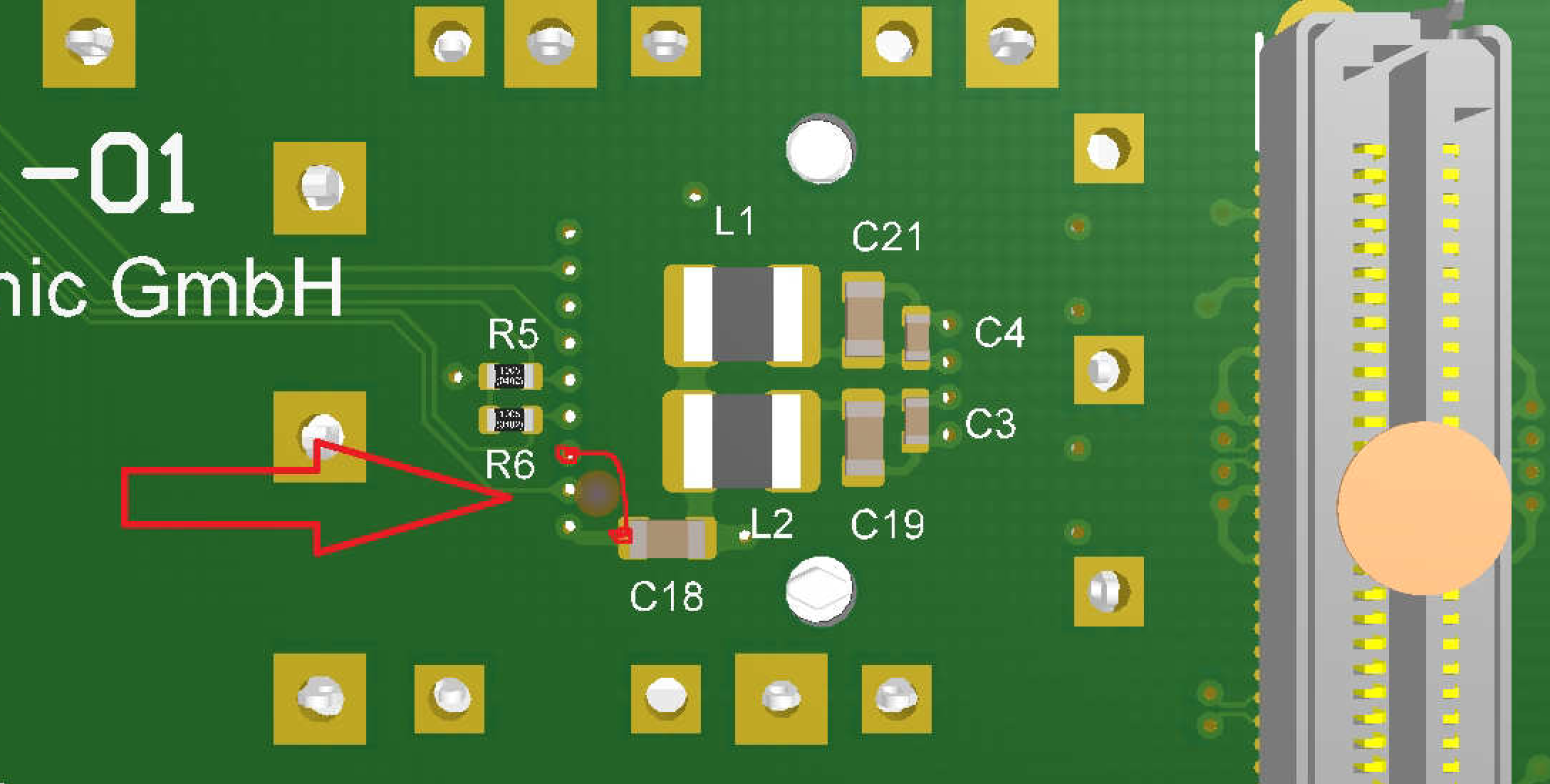
Figure 3: PCB wire patch for SFP+ connector.
Looped-backed MGT-Lanes on B2B Connector JB1 and JB2
The TEBA0841 carrier board is mainly designed for the 4 x 5 SoMs TE0841 and TE0741. This SoMs have GTX-Transceiver units on their FPGA-modules with up to 8 available MGT-lanes. To test this MGT-lanes, 5 RX/TX differential pairs are bridged on-board, hence the transmitted data on this MGT-lanes flows back to their sources in a loop-back circuit without intentional processing or modification.
The MGT lane pins are bridged on-board as fellows, if 4 x 5 SoM TE0741 is mounted on carrier board:
...
JB2-8 (MGT_TX0_N)
JB2-10 (MGT_TX0_P)
...
JB2-7 (MGT_RX0_N)
JB2-9 (MGT_RX0_P)
...
JB2-7 to JB2-8
JB2-9 to JB2-10
...
JB2-14 (MGT_TX1_N)
JB2-16 (MGT_TX1_P)
...
JB2-13 (MGT_RX1_N)
JB2-15 (MGT_RX1_P)
...
JB2-13 to JB2-14
JB2-15 to JB2-16
...
JB2-20 (MGT_TX2_N)
JB2-22 (MGT_TX2_P)
...
JB2-19 (MGT_RX2_N)
JB2-21 (MGT_RX2_P)
...
JB2-19 to JB2-20
JB2-21 to JB2-22
...
JB1-3 (MGT_TX7_P)
JB1-5 (MGT_TX7_N)
...
JB1-9 (MGT_RX7_P)
JB1-11 (MGT_RX7_N)
...
JB1-3 to JB1-9
JB1-5 to JB1-11
...
JB1-15 (MGT_TX6_P)
JB1-17 (MGT_TX6_N)
...
JB1-21 (MGT_RX6_P)
JB1-23 (MGT_RX6_N)
...
JB1-15 to JB1-21
JB1-17 to JB1-23
Ultra Small SMT Coaxial Connectors
4 HIROSE Ultra Small Surface Mount Coaxial Connectors (up to 6 Gbit/s transmission rate) are present on the Carrier Board available for access to one MGT lane of the SoM. The connectors have the manufacturer designation 'U.FL-R-SMT-1', mating hight: 2.4 mm.
Each conductor of the RX and TX differential pair is routed to one coaxial connector:
| Connector Designator | Connected to | B2B Connector |
|---|---|---|
| J5 | MGT_TX3_P | JM1-8 |
| J6 | MGT_TX3_N | JM1-10 |
| J7 | MGT_RX3_P | JM1-1 |
| J8 | MGT_RX3_N | JM1-3 |
Table 2: Pin-assignment of the coaxial connectors.
JTAG Interface
JTAG access to the mounted SoM is provided through B2B connector JB2 and is also routed to the XMOD header JX1 and pin header J3. With the TE0790 XMOD USB2.0 to JTAG adapter, the device of the mounted SoM can be programed via USB2.0 interface.
JTAG Signal | B2B Connector Pin | XMOD Header JX1 | Pin Header J3 | Note |
|---|---|---|---|---|
| TCK | JM1-90 | JX1-4 | J3-4 | - |
| TDI | JM1-86 | JX1-10 | J3-10 | - |
| TDO | JM1-88 | JX1-8 | J3-8 | - |
| TMS | JM1-92 | JX1-12 | J3-12 | - |
Table 5: JTAG interface signals.
XMOD FTDI JTAG-Adapter Header JX1
The JTAG interface of the mounted SoM can be accessed via XMOD header JX1, so in use with the XMOD-FT2232H adapter-board TE0790 the mounted SoM can be programmed via USB2.0 interface. The TE0790 board provides also an UART interface to the SoM's Zynq device which can be accessed by the USB2.0 interface of the adapter-board while the signals between these serial interfaces will be converted.
Following table describes the signals and interfaces of the XMOD header JX1:
| Pin Schematic Name | XMOD Header JX1 Pin | B2B | Note |
|---|---|---|---|
| TCK | C (pin 4) | JM1-90 | - |
| TDO | D (pin 8) | JM1-88 | - |
| TDI | F (pin 10) | JM1-86 | - |
| TMS | H (pin 12) | JM1-92 | - |
| B14_L25 | A (pin 3) | JM2-97 | UART-TX (transmit line) |
| B14_L0 | B (pin 7) | JM2-99 | UART-RX (receive line) |
| BOOTMODE | E (pin 9) | JM2-100 | - |
| PROG_B | G (pin 11) | JM1-94 | - |
Table 6: XMOD header JX1 signals and connections.
When using XMOD FTDI JTAG Adapter TE0790, the adapter-board's VCC and VCCIO will be sourced by the board's and module's 3.3V supply voltage. Set the XMOD DIP-switch with the setting:
| XMOD DIP-switches | Position |
|---|---|
| Switch 1 | ON |
| Switch 2 | OFF |
| Switch 3 | OFF |
| Switch 4 | OFF |
Table 7: XMOD adapter board DIP-switch positions for voltage configuration.
| Note |
|---|
Use Xilinx compatible TE0790 adapter board (designation TE-0790-xx with out 'L') to program the Xilinx Zynq devices. The TE0790 adapter board's CPLD have to be configured with the Standard variant of the firmware. Refer to the TE0790 Resources Site for further information and firmware download. |
JTAG/UART Header J3
As alternative to the XMOD header JX1, on the Carrier Board pin header J3 is present, which has a XMOD header-compatible pin-assignment, but also 4 additional pins as differential pairs to supply the mounted SoM with an external MGT reference clock signal and as differential analog signal input:
| Pin Schematic Name | Header J3 Pin | B2B | Note |
|---|---|---|---|
| TCK | 4 | JM1-90 | - |
| TDO | 8 | JM1-88 | - |
| TDI | 10 | JM1-86 | - |
| TMS | 12 | JM1-92 | - |
| B14_L25 | 3 | JM2-97 | UART-TX (transmit line) |
| B14_L0 | 7 | JM2-99 |
Table 4: Looped-backed MGT-lanes for mounted 4 x 5 SoM TE0741.
| Note |
|---|
| Note: The mounted TE 4 x 5 SoMs have different schematic net-names of the differential signaling pairs of the MGT-lanes. See Schematic of the particular SoM. |
JTAG Interface
JTAG access to the mounted SoM is provided through B2B connector JB2 and is also routed to the XMOD header JX1 and pin header J3. With the TE0790 XMOD USB2.0 to JTAG adapter, the device of the mounted SoM can be programed via USB2.0 interface.
...
JTAG Signal
...
B2B Connector Pin
...
Table 5: JTAG interface signals.
UART Interface
UART interface is available on B2B connector JB1 and is usually established by MIO-pins of the PS-bank of the mounted SoM's Zynq device. With the TE0790 XMOD USB2.0 adapter, the UART signals can be converted to USB2.0 interface signals:
| UART-RX (receive line) |
| BOOTMODE |
| 9 |
| JM2- |
| 100 |
| - |
Table 6: UART interface signals.
SD IO Interface
The SD IO interface of the mounted SoM is routed to the pin header J4. Due to the different operation voltage levels of the MicroSD Card socket (3.3V) and the and the SoM's Zynq device MIO-bank (1.8V), a VDD/VCCIO translation is necessary which can be provided for example by Texas Instruments TXS02612 SDIO port expander IC. Both voltage levels are available on pin header J4:
...
Table 7: SD IO interface signals.
USB2.0 Interface
TEBA0841 board has one physical Micro USB2.0 type B socket J10, the differential data signals of the USB2.0 socket are routed to the B2B connector JB2, where they can be accessed by the corresponding USB2.0 PHY transceiver of the mounted SoM.
With Micro USB2.0 type B socket, the USB2.0 interface can also be used in Device or OTG mode.
Following table gives an overview of the USB2.0 interface signals:
...
JB2-48
...
Table 8: USB2.0 interface signals and connections.
XMOD FTDI JTAG-Adapter Header
The JTAG interface of the mounted SoM can be accessed via XMOD header JX1 and pin header J3, which has a 'XMOD FTDI JTAG Adapter'-compatible pin-assignment, but also two additional pins (15,16) as differential pairs to supply the mounted SoM with an external MGT reference clock signal.
So in use with the XMOD-FT2232H adapter-board TE0790 the mounted SoM can be programmed via USB2.0 interface. The TE0790 board provides also an UART interface to the SoM's Zynq device which can be accessed by the USB2.0 interface of the adapter-board while the signals between these serial interfaces will be converted.
Following table describes the signals and interfaces of the XMOD header JX1 and pin header J3:
...
When using XMOD FTDI JTAG Adapter TE0790, the adapter-board's VCC and VCCIO will be sourced by the on-boards 3.3V supply voltage. Set the DIP-switch with the setting:
...
Use Xilinx compatible TE0790 adapter board (designation TE-0790-xx with out 'L') to program the Xilinx Zynq devices.
...
| PROG_B | 11 | JM1-94 | - |
| XADC_P | 13 | JM1-25 | Analog input differential pair |
| XADC_N | 14 | JM1-27 | |
| CLK0_N | 15 | JM1-4 | AC decoupled on-board (100 nF capacitor) |
| CLK0_P | 16 | JM1-2 |
Table 8: JTAG/UART header J3 signals and connections.
UART Interface
UART interface is available on B2B connector JM2. With the TE0790 XMOD USB2.0 adapter, the UART signals can be converted to USB2.0 interface signals:
| UART Signal Schematic Name | B2B | XMOD Header JX1 | Pin Header J3 | Note |
|---|---|---|---|---|
| B14_L0 | JM2-99 | JX1-7 | J3-7 | UART-RX (receive line) |
| B14_L25 | JM2-97 | JX1-3 | J3-3 | UART-TX (transmit line) |
Table 6: UART interface signals.
SD IO Interface
The SD IO interface of the mounted SoM is routed to the pin header J4. Due to the different operation voltage levels of the MicroSD Card socket (3.3V) and the and the SoM's Zynq device MIO-bank (1.8V), a VDD/VCCIO translation is necessary which can be provided for example by Texas Instruments TXS02612 SDIO port expander IC. Both voltage levels are available on pin header J4:
| SD IO Signal Schematic Name | B2B | Pin Header J4 | Note |
|---|---|---|---|
| SD_DAT0 | JB1-24 | J4-8 | SD IO data |
| SD_DAT1 | JB1-22 | J4-10 | SD IO data |
| SD_DAT2 | JB1-20 | J4-9 | SD IO data |
| SD_DAT3 | JB1-18 | J4-7 | SD IO data |
| SD_CLK | JB1-28 | J4-4 | SD IO clock |
| SD_CMD | JB1-26 | J4-3 | SD IO command |
Table 7: SD IO interface signals.
On-board Peripherals
| HTML |
|---|
<!-- Components on the Module, like Flash, PLL, PHY... --> |
...
Overview
Content Tools