Page History
...
Additional assembly options are available for cost or performance optimization upon request.
Block Diagram
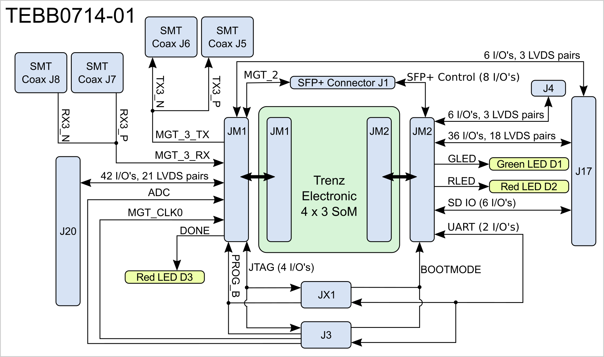
Figure 1: TEBB0714-01 Block Diagram.
...
Each conductor of the RX and TX differential pair is routed to one coaxial connector:
| Connector Designator | Connected to | B2B Connector |
|---|---|---|
| J5 | MGT_TX3_P | JM1-8 |
| J6 | MGT_TX3_N | JM1-10 |
| J7 | MGT_RX3_P | JM1-1 |
| J8 | MGT_RX3_N | JM1-3 |
Table 2: Pin-assignment of the coaxial connectors.
...
Following table describes the signals and interfaces of the XMOD header JX1:
| Pin Schematic Name | XMOD Header JX1 Pin | B2B | Note |
|---|---|---|---|
| TCK | C (pin 4) | JM1-90 | - |
| TDO | D (pin 8) | JM1-88 | - |
| TDI | F (pin 10) | JM1-86 | - |
| TMS | H (pin 12) | JM1-92 | - |
| B14_L25 | A (pin 3) | JM2-97 | UART-TX (transmit line) |
| B14_L0 | B (pin 7) | JM2-99 | UART-RX (receive line) |
| BOOTMODE | E (pin 9) | JM2-100 | - |
| PROG_B | G (pin 11) | JM1-94 | - |
Table 6: XMOD header JX1 signals and connections.
When using XMOD FTDI JTAG Adapter TE0790, the adapter-board's VCC and VCCIO will be sourced by the boardCarrier Board's and module's 3.3V supply voltage. Set the XMOD DIP-switch with the setting:
| XMOD DIP-switches | Position |
|---|---|
| Switch 1 | ON |
| Switch 2 | OFF |
| Switch 3 | OFF |
| Switch 4 | OFF |
Table 7: XMOD adapter board DIP-switch positions for voltage configuration.
| Note |
|---|
Use Xilinx compatible TE0790 adapter board (designation TE-0790-xx with out 'L') to program the Xilinx Zynq devices. The TE0790 adapter board's CPLD have to be configured with the Standard variant of the firmware. Refer to the TE0790 Resources Site for further information and firmware download. |
JTAG/UART Header J3
As alternative to the XMOD header JX1, on the Carrier Board pin header J3 is present, which has a XMOD header-compatible pin-assignment, but also 4 additional pins as differential pairs to supply the mounted SoM with an external MGT reference clock signal and as differential analog signal input:
The I/O-voltage of the XMOD adapter board with the schematic name 'V_CFG' and pin-name 'VIO' (pin 6) on XMOD header JX1 can be selected via Jumper J27:
V_CFG Value | Jumper J27 Setting | Note |
|---|---|---|
| 1.8V | pins 1-2 connected | Module's output voltage. |
| V_CFG0 | pins 3-4 connected | Internal module's VCCIO: 3.3V or 1.8V, depending on TE0714 module configuration. |
| 3.3V_OUT | pins 5-6 connected | Module's output voltage. |
Table 7: Setting of reference I/O-voltage XMOD header.
| Note |
|---|
Use Xilinx compatible TE0790 adapter board (designation TE-0790-xx with out 'L') to program the Xilinx Zynq devices. The TE0790 adapter board's CPLD have to be configured with the Standard variant of the firmware. Refer to the TE0790 Resources Site for further information and firmware download. |
JTAG/UART Header J3
As alternative to the XMOD header JX1, on the Carrier Board pin header J3 is present, which has a XMOD header-compatible pin-assignment, but also 4 additional pins as differential pairs to supply the mounted SoM with an external MGT reference clock signal and as differential analog signal input:
| Pin Schematic Name | Header J3 Pin | B2B | Note |
|---|
| TCK | 4 | JM1-90 | - |
| TDO | 8 | JM1-88 | - |
| TDI | 10 | JM1-86 | - |
| TMS | 12 | JM1-92 | - |
| B14_L25 | 3 | JM2-97 | UART-TX (transmit line) |
| B14_L0 | 7 | JM2-99 | UART-RX (receive line) |
| BOOTMODE | 9 | JM2-100 | - |
| PROG_B | 11 | JM1-94 | - |
| XADC_P | 13 | JM1-25 | Analog input differential pair |
| XADC_N | 14 | JM1-27 |
Table 8: JTAG/UART header J3 signals and connections.
UART Interface
UART interface is available on B2B connector JM2. With the TE0790 XMOD USB2.0 adapter, the UART signals can be converted to USB2.0 interface signals:
...
Table 6: UART interface signals.
SD IO Interface
The SD IO interface of the mounted SoM is routed to the pin header J4. Due to the different operation voltage levels of the MicroSD Card socket (3.3V) and the and the SoM's Zynq device MIO-bank (1.8V), a VDD/VCCIO translation is necessary which can be provided for example by Texas Instruments TXS02612 SDIO port expander IC. Both voltage levels are available on pin header J4:
...
| CLK0_N | 15 | JM1-4 | AC decoupled on-board (100 nF capacitor) |
| CLK0_P | 16 | JM1-2 |
Table 8: JTAG/UART header J3 signals and connections.
UART Interface
UART interface is available on B2B connector JM2. With the TE0790 XMOD USB2.0 adapter, the UART signals can be converted to USB2.0 interface signals:
| UART Signal Schematic Name | B2B | XMOD Header JX1 | Pin Header J3 | Note |
|---|---|---|---|---|
| B14_L0 | JM2-99 | JX1-7 | J3-7 | UART-RX (receive line) |
| B14_L25 | JM2-97 | JX1-3 | J3-3 | UART-TX (transmit line) |
Table 6: UART interface signals.
QSPI Interface
The QSPI interface (if available) of the mounted SoM is routed to the pin header J17. The reference I/O-voltage of the module have to be noticed when using this interface.
| SD IO Signal Schematic Name | B2B | Pin Header J17 | Note |
|---|---|---|---|
| SPI-DQO | JM2-68 | J17-24 | QSPI data |
| SPI-DQ1 | JM2-71 | J17-27 | QSPI data |
| SPI-DQ2 | JM2-73 | J17-28 | QSPI data |
| SPI-DQ3 | JM2-70 | J17-23 | QSPI data |
| SPI-CLK | JM2-67 | J17-26 | QSPI clock |
| SPI_CS | JM2-69 | J17-25 | QSPI chip select |
Table 7: QSPI interface signals.
On-board Peripherals
| HTML |
|---|
<!--
Components on the Module, like Flash, PLL, PHY...
--> |
On-board LEDs
The on-board LEDs are available to the user and can be used to indicate system status and activities:
| LED Designator | Color | Pin Schematic Name | B2B Connector | Indicating |
|---|---|---|---|---|
| D1 | green | GLED | JM2-26 | available to user |
| D2 | red | RLED | JM2-24 | available to user |
| D3 | red | DONE | JM1-96 | FPGA-modul programmed properly. |
Figure 11: On-board LEDs
VCCIO Selection Jumper
On the TEBB0714 Carrier Board the PL-bank I/O voltage (schematic name 'VCCIO34') can be selected by the jumper J26.
VCCIO34 Value | Jumper J26 Setting | Note |
|---|---|---|
| 1.8V | pins 1-2 connected | Module's output voltage. |
| 2.5V | pins 3-4 connected | Voltage generated by on-board LDO U1. |
| 3.3V_OUT | pins 5-6 connected | Module's output voltage. |
Table 12: Base-board PL-bank I/O voltage setting
Table 7: SD IO interface signals.
On-board Peripherals
| HTML |
|---|
<!--
Components on the Module, like Flash, PLL, PHY...
--> |
On-board LEDs
The on-board LEDs are available to the user and can be used to indicate system status and activities:
...
Figure 11: On-board LEDs
VCCIO Selection Jumper
On the TEBA0841 carrier board different VCCIO configurations can be selected by the jumper J26 and J27.
TE 4 x 5 Modules have a standard assignment of PL-bank I/O voltages on their B2B connectors, which will be fed with I/O voltage from base-board.
...
Base-board PL-bank I/O Voltages
...
Table 12: Base-board PL-bank I/O voltages VCCIOA and VCCIOD
| Note |
|---|
Note: The corresponding PL-bank I/O voltages of the 4 x 5 SoM to the selectable base-board voltages VCCIOA and VCCIOD are depending on the mounted 4 x 5 SoM and varying in order of the used model. Refer to the SoM's schematic for information about the specific pin assignments on module's B2B-connectors regarding the PL-bank I/O voltages and to the 4 x 5 Module integration Guide for VCCIO voltage options. |
Following table describes how to configure the base-board supply-voltages by jumpers:
...
Base-board PL-bank I/O Voltages
vs Voltage Levels
...
Table 13: Configuration of base-board supply-voltages via jumpers. Jumper-Notification: 'Jx: 1-2' means pins 1 and 2 are connected, 'Jx: 3-4' means pins 3 and 4 are connected, and so on.
| Note |
|---|
Take care of the VCCO voltage ranges of the particular PL IO-banks (HR, HP) of the mounted SoM, otherwise damages may occur to the FPGA. Therefore, refer to the TRM of the mounted SoM to get the specific information of the voltage ranges. It is recommended to set and measure the PL IO-bank supply-voltages before mounting of TE 4 x 5 3 module to avoid failures and damages to the functionality of the mounted SoM. |
...
The PL-bank I/O voltages 1.8V, 2.5V and 3.3V will be available after the mounted SoM's 3.3V voltage level has reached stable state on B2B-connector pins JM2JM1-10 83 and JM2-1254, meaning that all on-module voltages have become stable and module is properly powered up.
Following diagram shows the distribution of the external input voltage of nominal 3.3V to the components:
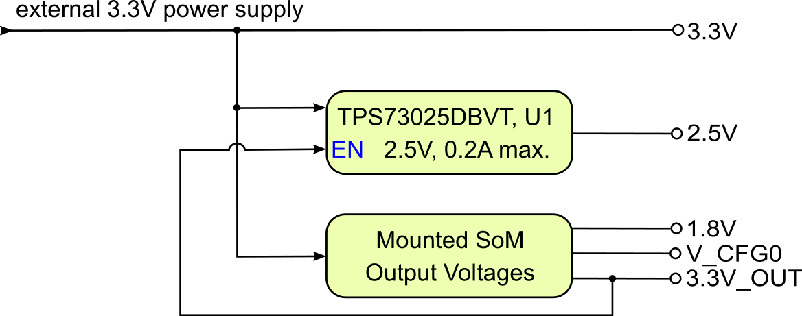
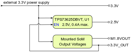
Figure 4: Board power distribution diagram.
...
Overview
Content Tools