Page History
...
| Scroll pdf ignore | |
|---|---|
Table of Contents
|
Overview
| Scroll Only (inline) |
|---|
Refer to https://shop.trenz-electronic.de/en/Download/?path=Trenz_Electronic/carrier_boards/TE0701 for downloadable version of this manual and additional technical documentation of the product. |
The Trenz Electronic TE0701 Carrier Board is a baseboard for 4 x 5 SoMs, which exposes the module's B2B connector pins to accessible connectors and provides a whole range of on-board components to test and evaluate TE 4 x 5 SoMs.
...
There are two baseboard supply voltages VIOTA and VIOTB connected to the 4 x 5 SoM's PL IO-bank. The supply-voltages have following pin assignments on B2B-connectors:
...
Table 4: Baseboard supply-voltages VIOTA and VIOTB
...
Baseboard supply voltages vs voltage levels | VIOTA | VIOTB | USB-VBUS | 12V0_CL |
|---|---|---|---|---|
| 3V3 | J17:1-2, 3 & J16: open | J17: 1-2, 3 & J16: open & J21:1-2, 3 | - | - |
| 2V5 | J17:1, 2-3 & J16: open | J17:1, 2-3 & J16: open & J21: 1-2, 3 | - | - |
| FMC_VADJ | J17: open & J16: 1-2 | J21:1, 2-3 | - | - |
| 5V0 intern | - | - | J9:1-2, 3 & J19: 1-2 (J20: 1-2: additional decoupling-capacitor 100 µF) | - |
| VBUS extern | - | - | J9: 1, 2-3 & J19: open | - |
| 12V_LC | - | - | - | J18: 1-2 |
Table 5: Configuration of baseboard supply-voltages via jumpers. 'Jx: 1-2, 3' means pins 1 and 2 are closed, pin 3 is open. 'Jx: 1, 2-3' means pins 2 and 3 are closed, pin 1 is open.
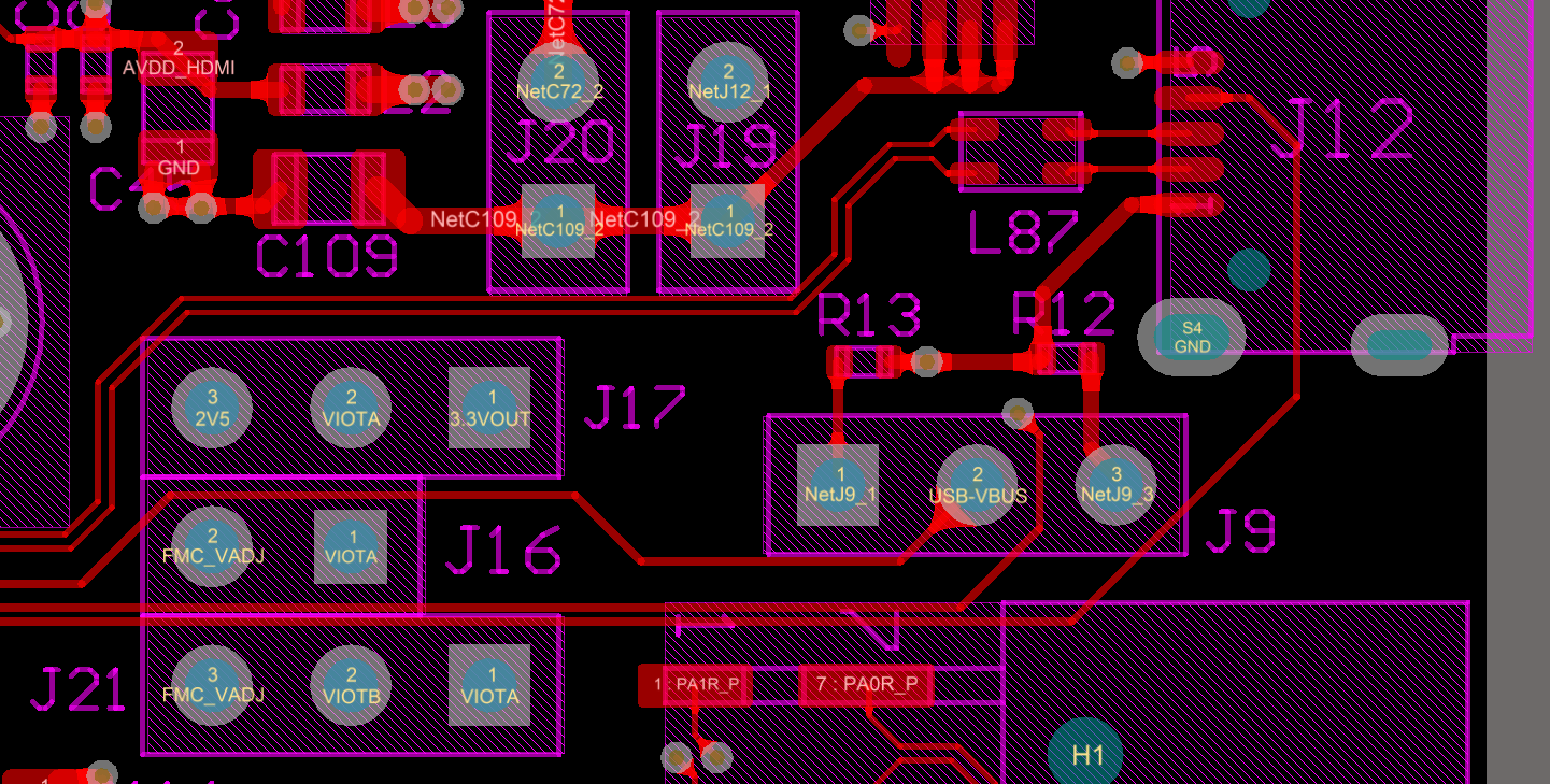
Figure 4: VCCIO jumper pin location (PCB-REV06), top view.
| Note |
|---|
Take care of the VCCO voltage ranges of the particular PL IO-banks (HR, HP) of the mounted SoM, otherwise damages may occur to the FPGA. Therefore, refer to the TRM of the mounted SoM to get the specific information of the voltage ranges. It is recommended to set and measure the PL IO-bank supply-voltages before mounting of TE 4 x 5 module to avoid failures and damages to the functionality of the mounted SoM. |
Board to Board Connectors
| Include Page | ||||
|---|---|---|---|---|
|
Technical Specifications
Absolute Maximum Ratings
...
ca. 188 g - Plain board.
Document Change History
| Date | Revision | Authors | Description | ||||||||
|---|---|---|---|---|---|---|---|---|---|---|---|
| John Hartfiel |
| |||||||||
| 2017-08-15 | v.59 | John Hartfiel |
| ||||||||
| 2017-08-14 | v.58 | John Hartfiel |
| ||||||||
| 2017-05-25 | v.56 | Jan Kumann |
| ||||||||
| 2017-05-16 | v.51 | Jan Kumann |
| ||||||||
| 2017-04-11 |
| Ali Naseri |
| ||||||||
| 2017-02-15 | v.45 | Ali Naseri |
| ||||||||
| 2017-02-15 | v.40 | Ali Naseri |
| ||||||||
| 2017-01-19 | v.35 | Ali Naseri |
| ||||||||
| 2017-01-13 | v.20 | Ali Naseri |
| ||||||||
| 2016-11-29 | v.10
| Ali Naseri |
| ||||||||
| 2016-11-28 | v.4 | Ali Naseri |
| ||||||||
| 2014-02-18 | 0.2 | Sven-Ole Voigt |
| ||||||||
| 2014-01-05 | 0.1 | Sven-Ole Voigt |
| ||||||||
| All | Sven-Ole Voigt, Ali Naseri |
Hardware Revision History
...
Overview
Content Tools