Page History
...
| Scroll pdf ignore | |
|---|---|
Table of Contents
|
Overview
| HTML |
|---|
<!-- Wiki Link: Go to Base Folder of the Module or Carrier, for example : https://wiki.trenz-electronic.de/display/PD/TE0712 --> |
...
The Trenz Electronic TEM0001 is a low cost small-sized FPGA module integrating a Microsemi SmartFusion2 FPGA SoC and 8 MByte Flash memory for configuration and operation.
Key Features
Microsemi SmartFusion2 SoC FPGA
- 8 MByte SDRAM
8 MByte QSPI Flash memory
- 25 MHz system clock and 32.768 KHz auxiliary clock
- JTAG and UART over Micro USB2 connector
- 1x 3-pin header for Live Probes
- 1x PMOD header providing 8 GPIOs
2x 14-pin headers (2,54 mm pitch) providing 23 GPIOs
9 user LEDs
- 1 user push button
- 3.3V single power supply with on-board voltage regulators
- Size 61.5 x 25 mm
Additional assembly options are available for cost or performance optimization upon request.
Block Diagram
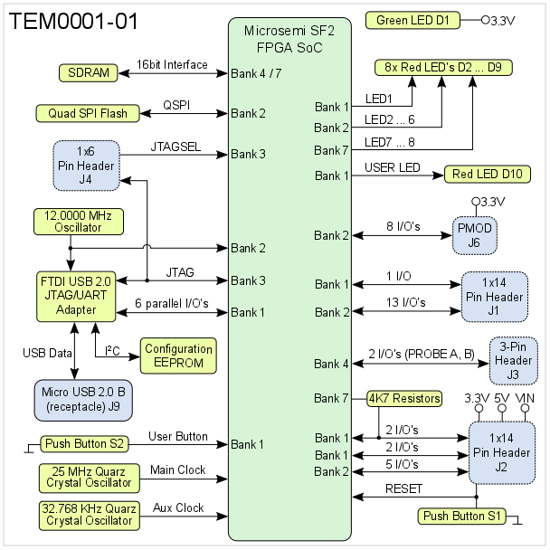
Figure 1: TEM0001-01 block diagram
Main Components
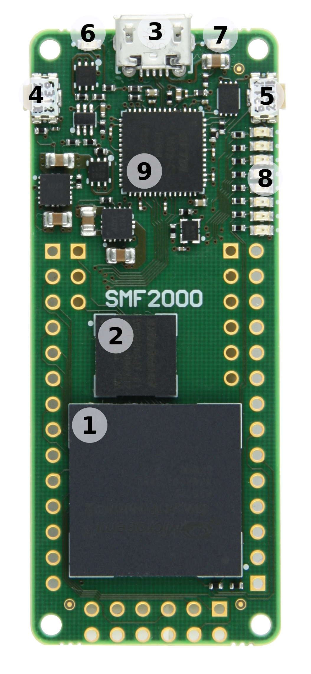
Figure 2: TEM0001-01 FPGA module
- Microsemi SmartFusion2 FPGA SoC, U5
- 8 Mbyte SDRAM 166MHz, U2
- Micro USB2 B socket (receptacle), J9
- Switch button (reset), S1
- Switch button (user), S2
- Red LED (user), D10
- Green LED (indicating supply voltage), D1
- 8x red LEDs (user), D2 - D9
- FTDI USB2 to JTAG/UART adapter, U3
- 8 Mbyte QSPI Flash memory, U1
- 32.768 KHz auxiliary crystal oscillator, Y1
- 25 MHz main crystal oscillator, Y2
- 1x14 pin header (2.54mm pitch), J2
- 1x6 pin header (2.54mm pitch), J4
- 3-pin header (2.54mm pitch), J3
- 1x14 pin header (2.54mm pitch), J1
- 2x6 Pmod connector, J6
Initial Delivery State
Storage device name | Content | Notes |
|---|---|---|
Quad SPI Flash (U1) OTP area | Empty | - |
| I2C Configuration EEPROM, U9 | Empty | - |
Table 1: Initial delivery state of programmable devices on the module
Boot Process
By default the configuration mode pins of the FPGA are set to QSPI mode, hence the FPGA is configured from serial NOR flash at system start-up. The JTAG interface of the module is provided for storing the initial FPGA configuration data to the QSPI flash memory.
Signals, Interfaces and Pins
I/Os on Pin Headers and Connectors
I/O signals of the FPGA SoC's I/O banks connected to the board's pin headers and connectors:
...
Table 2: General overview of PL I/O signals connected to pin headers and connectors
Single ended I/O banks
| Bank | VCCIO | I/O's Count | Available on Connectors | Notes |
|---|---|---|---|---|
| 1 | 3.3V | 14 | 5 | 6 I/O's connected to FTDI chip, 1 I/O used for user button S2, 2 I/O's connected to red user LEDs D2 and D10. |
| 2 | 3.3V | 37 | 26 | 6 I/O's user for QSPI Flash, 5 I/O's connected to red user LEDs D3 ... D7. |
| 3 | 3.3V | 5 | 5 | Bank 3 is dedicated to JTAG interface. |
| 4 | 3.3V | 24 | 0 | 2 I/O's are dedicated to live probes, all other I/O's are used as memory interface. |
| 7 | 3.3V | 22 | 2 | 2 I/O's available on header J2, 2 I/O's connected to red user LEDs D8 and D9, all other I/O's are used as memory interface. |
Table 3: General overview of single ended I/O banks
JTAG Interface
JTAG access to the FPGA SoC device U5 is provided through Micro USB2 B connector J9. The JTAG interface is created by the FTDI FT2232H USB2 to JTAG/UART adapter IC U3.
...
Table 4: JTAG interface signals
QSPI Interface
The QSPI interface of the FPGA device is routed to and used by the on-module QSPI flash IC U1:
...
Table 5: QSPI interface signals
On-board Peripherals
Quad SPI Flash Memory
On-module QSPI flash memory (U7) is provided by Winbond Serial NOR Flash Memory W74M64FV with 64 MBit (8 MByte) storage capacity. This non volatile memory is used to store initial FPGA configuration. Besides FPGA configuration, remaining free flash memory can be used for user application and data storage. All four SPI data lines are connected to the FPGA allowing x1, x2 or x4 data bus widths. Maximum data rate depends on the selected bus width and clock frequency used.
SDRAM
The TEM0001 FPGA module is equipped with a Winbond W9864G6JT 64 MBit (8 MByte) SDRAM IC U2. This SDRAM IC is connected to the FPGA bank 4 and 7 via 16bit memory interface with 166MHz clock frequency and CL3 CAS latency.
FTDI FT2232H IC
The FTDI chip U3 converts signals from USB2.0 to a variety of standard serial and parallel interfaces. Refer to the FTDI data sheet to get information about the capacity of the FT2232H IC.
FTDI FT2232H IC is used in MPPSE Mode for JTAG, 6 I/O's of Channel B are routed to the bank 1 of the FPGA SoC and are usable as for example UART and other standard serial or parallel interfaces. The configuration of FTDI FT2232H IC can be stored to and loaded from to the configuration EEPROM U9, which is not programmed on delivery state.
System Clock Oscillator
The FPGA SoC module has following reference clocking signals provided by on-board oscillators:
...
Table 6: Clock sources overview
On-board LEDs
There are 10 LEDs fitted on the FPGA module board. The LEDs are user configurable to indicate for example any system status.
...
Table 7: LEDs of the module
Push Buttons
The TEM0001 FPGA module is equipped with two push buttons S1 and S2:
...
Table 8: Push buttons of the module
Connectors
All connectors are are for 100mil headers, all connector locations are in 100mil (2.54mm) grid. The module's PCB provides footprints to mount and solder optional pin headers, if those are not factory-fitted on module.
Power and Power-On Sequence
To power-up a module, power supply with minimum current capability of 1A is recommended.
Power Supply
The FPGA module can be power-supplied through Micro USB2 connector J9 with supply voltage 'USB-VBUS' or alternative through pin header J2 with supply voltage 'VIN'.
...
Figure 3: Power Distribution Diagram
Power Consumption
| FPGA | Design | Typical Power, 25C ambient |
|---|---|---|
| Mircosemi SmartFusion2 FPGA SoC M2S010-VFG400 | Not configured | TBD* |
...
Actual power consumption depends on the FPGA design and ambient temperature.
Power-On Sequence
There is no specific or special power-on sequence, just one single power source is needed.
Technical Specifications
Absolute Maximum Ratings
Parameter | Min | Max | Units | Reference document |
|---|---|---|---|---|
VIN supply voltage (5.0V nominal) | -0.3 | 6.0 | V | EP53A7HQI / EP53A7LQI datasheet |
| I/O Input voltage for FPGA I/O bank | -0.3 | 3.63 | V | Microsemi datasheet DS0128 |
Storage Temperature | -40 | +90 | °C | LED R6C-AL1M2VY/3T datasheet |
Table 10: Absolute maximum ratings
Recommended Operating Conditions
| Parameter | Min | Max | Units | Reference document |
|---|---|---|---|---|
| VIN supply voltage (5.0V nominal) | 4.75 | 5.25 | V | same as USB-VBUS specification |
| I/O Input voltage for FPGA I/O bank | -0.3 | 3.45 | V | Microsemi datasheet DS0128 |
| Operating temperature range | 0 | +70 | °C | Winbond datasheet W9864G6GT |
...
| Note |
|---|
| Please check Microsemi datasheet DS0128 for complete list of absolute maximum and recommended operating ratings for the FPGA device. |
Physical Dimensions
Please note that two different units are used on the figures below, SI system millimeters (mm) and imperial system thousandths of an inch(mil). This is because of the 100mil pin headers used, see also explanation below. To convert mils to millimeters and vice versa use formula 100mil's = 2,54mm.
...
Figure 4: Module physical dimensions drawing
Revision History
Hardware Revision History
| Date | Revision | Notes | PCN | Documentation Link |
|---|---|---|---|---|
| - | 01 |
| - | TEM0001-01 |
...
Figure 5: Module hardware revision number
Document Change History
| Date | Revision | Contributors | Description | ||||||||
|---|---|---|---|---|---|---|---|---|---|---|---|
| Ali Naseri |
|
Table 13: Document change history
Disclaimer
| Include Page | ||||
|---|---|---|---|---|
|
Overview
Content Tools