Page History
...
| HTML |
|---|
<!-- Wiki Link: Go to Base Folder of the Module or Carrier, for example : https://wiki.trenz-electronic.de/display/PD/TE0712 --> |
The Trenz Electronic TEF0008 is a FPGA to Mezzanine Card (FMC) based on VITA 57.1 FMC HPC Standard, with four SFP+ 10Gb ports for fiber optical (850nm) portsSFP modules. It is inteded for use on a FMC HPC carrier and can not be used stand-alone.
| Scroll Only (inline) |
|---|
Refer to http://trenz.org/tef0008-info for the current online version of this manual and other available documentation.
|
Key Features
- Four SFP+ 10Gb (850nm) ports
- HPC FMC connector
- Low jitter programmable clock generator
- Intel(Altera) Max10 FPGA 10M08SAU169C8G
- Status LED (green)
Block Diagram

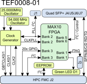
Figure 1: TEF0008 -01 block diagram.
Main Components
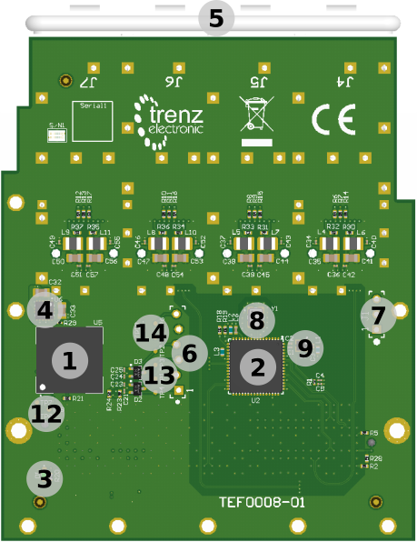
Figure 2: TEF0008 -01 FMC overview.
Table 1: TEF0008 -01 main components.
- MAX10 FPGA, U5
- Programmable low jitter clock generator Si5354A, U2
- Status LED (green), D1
- 3.3V to 1.8V DCDC converter, U6
- Quad SFP+ cage and connectors, J4-J7
- 1x6 pin header for JTAG programming of FPGA (3.3V), J3
- 1x3 pin header for I²C (1.8V), J1
- XTAL 54.0000 MHz (CX3225SB), Y1
- Oszillator 25.000000 MHz (SiT8008B), U1
- HPC FMC connector, J2
- 128KBit EEPROM, U4
- Testpoints Max10, TP7-TP9
- Testpoints JTAG, TP1-TP4
- Testpoints Power, TP5, TP6, TP10
...
Storage device name | Content | Notes | ||
|---|---|---|---|---|
Max10 FPGA 10M08SAU169C8G.. | Programmed | U5. Level shifter and controlller functions. | ||
Clock generator Si5345A-B-GM | Programmed | U2. ..OUT0 25MHz, OUT2 125MHz, OUT7 156.25 MHz, OUT8 156.25MHz, OUT9 125MHz. | ||
EEPROM | .. | 24LC128-I/ST | empty | U4, IPMI and VITA57.1 compatible.. |
Table 21: Initial delivery state of programmable devices on the module.
...
The MAX10 FPGA boots form its internal configuration flash memory, which is programmable via JTAG (J3).
Signals, Interfaces and Pins
...
| Bank | Type | B2B Connector | I/O Signal Count | Bank Voltage | Notes |
|---|---|---|---|---|---|
| 3 | GPI/Os | J2 | 20 I/Os | VADJ | Supplied by the carrier board. |
Table 32: General overview of I/O signals connected to the B2B connectors.
...
| Lane | SFP+ | Signal Name | HPC FMC Pin |
|---|---|---|---|
| 0 | J4 |
|
|
| 1 | J5 |
|
|
| 2 | J6 |
|
|
| 3 | J7 |
|
|
Table 43: MGT lanes.
Below are listed MGT banks reference clock sources.
| Clock signal | Source | HPC FMC Pin | Notes |
|---|---|---|---|
| GBTCLK0_P | U2-51 | J2-D4, GBTCLK0_M2C_P | On-board Si5345A. |
| GBTCLK0_N | U2-50 | J2-D5, GBTCLK0_M2C_N | On-board Si5345A. |
| GBTCLK1_P | U2-31 | J2-B20, GBTCLK1_M2C_P | On-board Si5345A. |
| GBTCLK1_N | U2-30 | J2-B21, GBTCLK1_M2C_N | On-board Si5345A. |
Table 54: MGT reference clock sources.
SFP+ Control Interface
Follwowing Following table contains a brief description of the control and status signals of the SFP+ connectors:
| Signal Schematic Name | FPGA Direction | Description | Logic |
|---|---|---|---|
| SFPx_TX_DISABLE | Output | SFP Enabled / Disabled | Low active |
| SFPx_LOS | Input | Loss of receiver signal | High active |
| SFPx_RS0 | Output | Full RX bandwidth | Low active |
| SFPx_RS1 | Output | Reduced RX bandwidth | Low active |
| SFPx_M-DEF0 | Input | Module present / not present | Low active |
| SFPx_TX_FAULT | Input | Fault / Normal Operation | High active |
| SFPx_SDA | BiDir | 2-wire Serial Interface Data | - |
| SFPx_SCL | Output (BiDir) | 2-wire Serial Interface Clock | - |
Table 5: Overview of SFP control Signals.
| Note |
|---|
Up to 100kHz the modules operate without clock streching. Therfore SCL can be implemented as driven by Master only. |
JTAG Interface
JTAG access to the MAX10 FPGA is provided through HPC FMC Connector and an additional pin header connector as well as testpoints.
...
Table 6: JTAG interface signals.
| HTML |
|---|
<!-- For the detailed function of the pins and signals, the internal signal assignment and implemented logic, look to the Wiki reference page SC CPLD of this module or into the bitstream file of the SC CPLD. Add link to the Wiki reference page of the SC CPLD, if available. --> |
I2C Interface
OnDespite the EEPROM U4 all other on-board I2C devices are connected to the HPC FMC Pin C30 SCL and pin C31 SDA which are reserved for I2C. Level shift and for PLL and SFP+ I²C is done by the FPGA as well as MUX for SFP+. Addresses for on-board MAX10 FPGA for level shift and I²C MUX. Addresses for devices are listed in the table below:. The EEPROM is accessed via the FMC connector.
| I2C Device | I2C Address | Notes |
|---|---|---|
| J4, SFP+ | 1100010 1100001 / 1100000 | Conventional SFP Memory / Enhanced Feature Set Memory, SFP Device select via MAX10 FPGA implementation. |
| J5, SFP+ | 1100010 1100001 / 1100000 | Conventional SFP Memory / Enhanced Feature Set Memory, SFP Device select via MAX10 FPGA implementation. |
| J6, SFP+ | 1100010 1100001 / 1100000 | Conventional SFP Memory / Enhanced Feature Set Memory, SFP Device select via MAX10 FPGA implementation. |
| J7, SFP+ | 1100010 1100001 / 1100000 | Conventional SFP Memory / Enhanced Feature Set Memory, SFP Device select via MAX10 FPGA implementation. |
| U2, Si5345A | 1101001 | Level shifted via MAX10 FPGA, Device select via MAX10 FPGA implementation. |
| U4, EEPROMU4, EEPROM | 10100xx | Last digits determined by carrier board via HPC FMC (C34 GA0, C35 GA1). |
Table 7: I2C slave device addresses.
On-board Peripherals
| HTML |
|---|
<!--
Components on the Module, like Flash, PLL, PHY...
--> |
Programmable Clock Generator
There is a Silicon Labs I2C programmable clock generator on-board (Si5345A, U2) to generate reference clocks for the module.
Not connected.
...
IN0
...
Reference input clock.
...
IN2
...
-
...
IN3
...
A1
...
-
...
OUT0
...
CLKPLL2F
...
FPGA bank 2.
...
-
...
Not connected.
...
Output
...
Table 8: Programmable clock generator inputs and outputs.
Oscillators
The module has following reference clock signals provided by on-board oscillators and external source from carrier board:
...
HPC FMC Connector
The following table lists all on the FMC connector assigned net names.
| A | B | C | D | E | F | G | H | J | K | |
|---|---|---|---|---|---|---|---|---|---|---|
| 1 | GND | NetJ2_B1 | GND | PG_C2M | GND | PG_M2C | GND | GND | ||
| 2 | SFPB_RD_P | GND | SFPA_TD_P | GND | GND | CLK1_P | GND | GND | ||
| 3 | SFPB_RD_N | GND | SFPA_TD_N | GND | GND | CLK1_N | GND | GND | ||
| 4 | GND | GND | GBTCLK0_P | GND | GND | CLK0_P | GND | CLK2_P | ||
| 5 | GND | GND | GBTCLK0_N | GND | GND | CLK0_N | GND | CLK2_N | ||
| 6 | SFPC_RD_P | GND | SFPA_RD_P | GND | GND | LA00_P | GND | GND | ||
| 7 | SFPC_RD_N | GND | SFPA_RD_N | GND | LA00_N | LA02_P | ||||
| 8 | GND | GND | LA01_P | GND | GND | LA02_N | GND | |||
| 9 | GND | GND | LA01_N | GND | LA03_P | GND | GND | |||
| 10 | SFPD_RD_P | GND | LA06_P | GND | LA03_N | LA04_P | ||||
| 11 | SFPD_RD_N | GND | LA06_N | LA05_P | GND | GND | LA04_N | GND | ||
| 12 | GND | GND | LA05_N | GND | LA08_P | GND | GND | |||
| 13 | GND | GND | GND | LA08_N | LA07_P | |||||
| 14 | GND | LA09_P | GND | GND | LA07_N | GND | ||||
| 15 | GND | LA09_N | GND | GND | GND | |||||
| 16 | GND | GND | GND | |||||||
| 17 | GND | GND | GND | GND | GND | |||||
| 18 | GND | GND | GND | GND | ||||||
| 19 | GND | GND | ||||||||
| 20 | GND | GBTCLK1_P | GND | GND | GND | GND | ||||
| 21 | GND | GBTCLK1_N | GND | GND | GND | GND | ||||
| 22 | SFPB_TD_P | GND | GND | |||||||
| 23 | SFPB_TD_N | GND | GND | GND | GND | |||||
| 24 | GND | GND | GND | GND | GND | |||||
| 25 | GND | GND | GND | |||||||
| 26 | SFPC_TD_P | GND | GND | GND | GND | |||||
| 27 | SFPC_TD_N | GND | GND | GND | GND | |||||
| 28 | GND | GND | GND | |||||||
| 29 | GND | GND | TCK | GND | GND | GND | ||||
| 30 | SFPD_TD_P | GND | FMC_SCL | TDI | GND | GND | GND | |||
| 31 | SFPD_TD_N | GND | FMC_SDA | TDO | ||||||
| 32 | GND | GND | 3P3VAUX | GND | GND | GND | ||||
| 33 | GND | GND | TMS | GND | GND | GND | ||||
| 34 | GND | GA0 | ||||||||
| 35 | GND | 12V | GA1 | GND | GND | GND | ||||
| 36 | GND | GND | 3P3V | GND | GND | GND | ||||
| 37 | GND | 12V | GND | |||||||
| 38 | GND | GND | 3P3V | GND | GND | GND | ||||
| 39 | GND | 3P3V | GND | VADJ | GND | VADJ | GND | GND | ||
| 40 | GND | GND | 3P3V | GND | VADJ | GND | VADJ | GND |
Table 8: HPC FMC Connector pin assignment.
On-board Peripherals
| HTML |
|---|
<!--
Components on the Module, like Flash, PLL, PHY...
--> |
MAX10 FPGA
The MAX10 FPGA (10M08SAU169C8G) is used as SFP control, level shifter and I2C MUX. For a detailed description see TEF0008 MAX10.
Programmable Clock Generator
There is a Silicon Labs I2C programmable clock generator on-board (Si5345A, U2) to generate reference clocks for the module. Programming can be done using I2C via PIN header J1. The I2C bus is also routed to the MAX10 FPGA.
| Si5345A Pin | Signal Name / Description | Connected To | Direction | Note | Default |
|---|---|---|---|---|---|
IN0 | Reference input clock. | U1 | Input | 25.000000 MHz oscillator, Si8208AI | |
| IN1 | - | Not connected. | Input | Not used. | |
IN2 | - | Not connected. | Input | Not used. | |
IN3 | CLK2 | J2-K4/K5 | Input | HPC FMC configured as C2M clock. | |
A1 | - | GND | Input | I2C slave device address LSB. | |
| XAXB | - | Y1 | Input | 54.0000 MHz XTAL CX3225SB | |
OUT0 | CLKPLL2F | U5-H6/G5 | Output | FPGA bank 2. | 25MHz |
| OUT1 | - | Not connected. | Output | Not used. | --- |
| OUT2 | GBTCLK1 | J2-B20/B21 | Output | M2C via HPC FMC. | 125MHz |
| OUT3 | - | Not connected. | Output | Not used. | --- |
| OUT4 | - | Not connected. | Output | Not used. | --- |
| OUT5 | - | Not connected. | Output | Not used. | --- |
| OUT6 | - | Not connected. | Output | Not used. | --- |
| OUT7 | GBTCLK0 | J2-D4/D5 | Output | M2C via HPC FMC. | 156.25MHz |
| OUT8 | CLK0 | J2-H4/H5 | Output | M2C via HPC FMC. | 156.25MHz |
| OUT9 | CLK1 | J2-G2/G3 | Output | M2C via HPC FMC. | 125MHz |
Table 9: Programmable clock generator inputs and outputs.
Oscillators
The module has following reference clock signals provided by on-board oscillators and external source from carrier board:
| Clock Source | Schematic Name | Frequency | Clock Destination |
|---|---|---|---|
| SiTime SiT8008AI oscillator, U1 | - | 25.000000 MHz | U2-63/64 |
| Carrier board via HPC FMC J2-K4/K5 | CLK2 | Defined by carrier. | U2-61/62 |
Table 10: Reference clock signals.
EEPROM
A Microchip 24LC128-I/LC serial EEPROM (U4) is provided for IPMI data. It is accessible via the LPC FMC connector (SCL C30, SDA C31).
On-board LED
Table 9: Reference clock signals.
EEPROM
A Microchip 24AA025E48 serial EEPROM (U23) contains a globally unique 48-bit node address, which is compatible with EUI-48(TM) specification. The device is organized as two blocks of 128 x 8-bit memory. One of the blocks stores the 48-bit node address and is write protected, the other block is available for application use. It is accessible over I2C bus with slave device address 0x53.
...
| LED | Color | Connected to | Description and Notes | |
|---|---|---|---|---|
| D1 | Green | U5-C2 (bank 1A) | Status LED: ... | Depending on FPGA design. With the shipped FPGA design it is on, if at least one SFP is connected. |
Table 11Table 10: On-board LEDsLED.
Power and Power-On Sequence
...
| 3P3V | TBD* |
| VADJ (at 1.8V) | TBD* |
3P3VAUX | TBD* |
Table 1112: Typical power consumption.
...
Power Distribution Dependencies
...
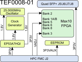
Figure 3: Module power distribution diagram.
...
Power Rail Name | HPC FMC Connector (J2) | Direction | Notes |
|---|---|---|---|
| 3P3V | D36, D38, D40, C39 | Input | Supply voltage from carrier board. |
| 1.8V | - | Output | Module on-board 1.8V voltage supply (Max 1A). |
3P3VAUX | D32 | Input | Supply voltage from carrier board. |
VADJ | H40, G39, F40, E39 | Input | Supply voltage from carrier board. |
| 12V | C35, C37 | Input | Not used supply voltage from carrier board. |
Table 1213: Module power rails.
Bank Voltages
Bank | Schematic Name | Voltage | Voltage Range |
|---|---|---|---|
| 1A | 3P3V | 3.3V | - |
| 1B | 3P3V | 3.3V | - |
| 2 | 1.8V | 1.8V | - |
| 3 | VADJ | Carrier supplied | 1.2V - 3.3V |
| 5 | 3P3V | 3.3V | - |
| 6 | 3P3V | 3.3V | - |
| 8 | 3P3V | 3.3V | - |
Table 1314: Module PL I/O bank voltages.
Variants Currently In Production
...
Operating Temperature
...
.
Variants Currently In Production
| Module Variant | FPGA | Operating Temperature | Temperature Range |
|---|---|---|---|
| TE0008-02 | 10M08SAU169C8G | 0°C to +85°C | Extended |
Table 14: Module variants.
Technical Specifications
Absolute Maximum Ratings
Parameter | Min | Max | Units | Reference Document |
|---|---|---|---|---|
VIN supply voltage | V | - | ||
Storage temperature |
| °C | -
Table 15: Module absolute maximum ratings.
...
variants.
Technical Specifications
Absolute Maximum Ratings
Parameter | Min | Max | Units |
|---|
Reference Document | ||||
|---|---|---|---|---|
Storage temperature | -40 | 85 | °C | - |
Table 16: Module recommended operating conditionsabsolute maximum ratings.
Operating Temperature Ranges
Commercial Extended grade: 0°C to +70°C85°C.
Physical Dimensions
Module size: 69 mm × 84 mm, SFP+ conector excluded (+ 5.5 mm). See Vita 57.1 standard.
PCB thickness: 1.6 mm.
Highest part on PCB top is 9.5 mm (SFP+ cage, excluded front plate), bottom 1.4 mm (MAX10 FPGA). Please download the step model for exact numbers.
All dimensions are given in millimeters.
Put mechanical drawings here...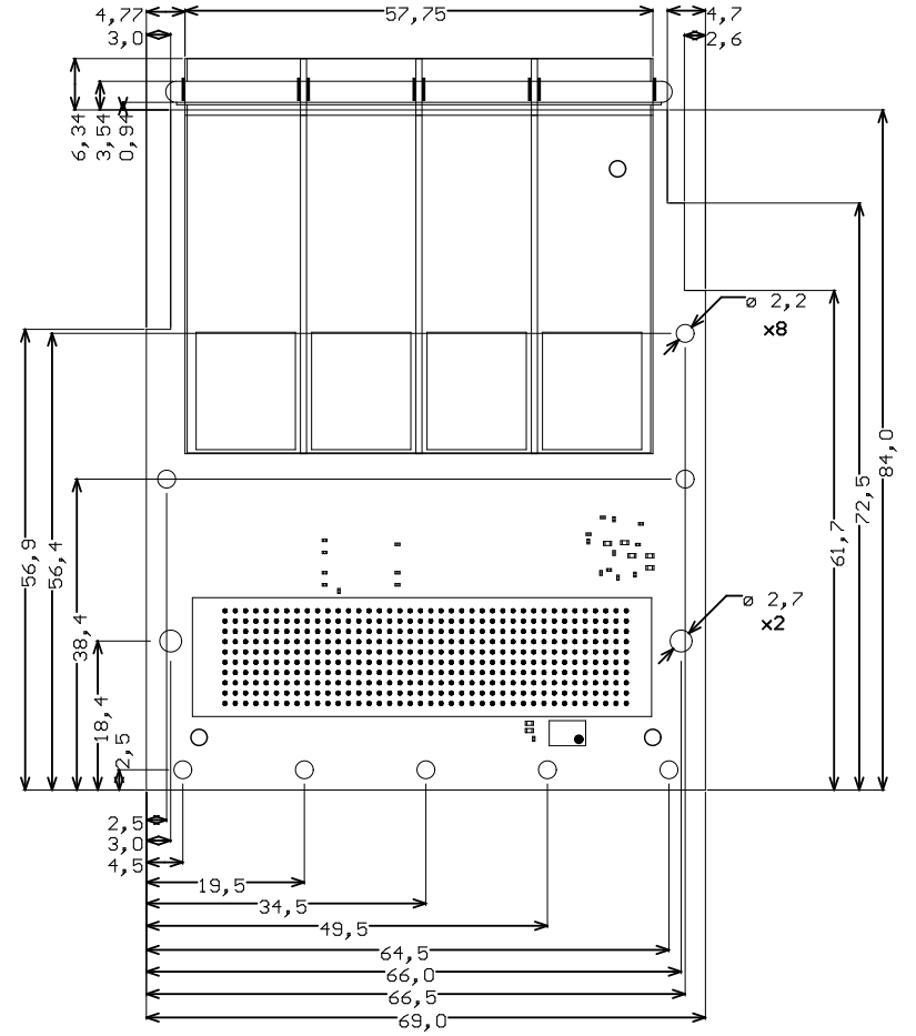
Figure 4: Module physical dimensions drawing.
| Note |
|---|
Mounting holes near the front pannel are not implemented due to physical restrictions caused by the SFP cage. The dimensions exceed in some area the by Vita 57.1 standard defined dimensions. In the middle region of the card the cage is higher than the specified max high for this area. Check carefully if the carrier card uses this space for other components conflicting mechanical. The bottom side is at the high limit. |
...
| Date | Revision | Notes | PCN | Documentation Link | ||
|---|---|---|---|---|---|---|
| 2018-06-06 | 02 | 01 | First production release | |||
| - | 01 | Prototypes |
Table 17: Module hardware revision history.
...
Hardware revision number can be found on the PCB board together with the module model number separated by the dash.
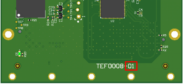
Figure 45: Module hardware revision number.
...
| HTML |
|---|
<!-- Generate new entry: 1.add new row below first 2.Copy "Page Information Macro(date)" Macro-Preview, Metadata Version number, Author Name and description to the empty row. Important Revision number must be the same as the Wiki document revision number 3.Update Metadata = "Page Information Macro "Page Information Macro (current-version)" Preview+1 and add Author and change description. -->(current-version)" Preview+1 and add Author and change description. --> |
Date | Revision | Contributors | Description | ||||||||||||||||||||||||||
|---|---|---|---|---|---|---|---|---|---|---|---|---|---|---|---|---|---|---|---|---|---|---|---|---|---|---|---|---|---|
|
|
|
| ||||||||||||||||||||||||||
| 2018-08-24 | v.38 | Martin Rohrmüller |
| ||||||||||||||||||||||||||
2018-06-15 | Martin Rohrmüller |
| |||||||||||||||||||||||||||
| --- | all |
|
|
Date
Revision
Contributors
Description
Martin Rohrmüller
Initial document.
all
Jan Kumann, John Hartfiel
Table 18: Document change history.
...
Overview
Content Tools