Page History
...
- VITA 57.1 FMC HPC standard compatible
- Four SFP+ 10Gb (850nm) ports
- Low jitter programmable clock generator
- Intel(Altera) Max10 FPGA 10M08SAU169C8G
- Status LED (green)
Block Diagram

Figure 1: TEF0008-01 block diagram.
Main Components
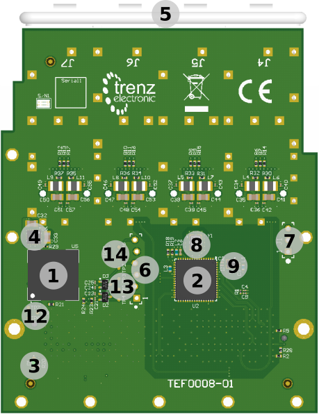
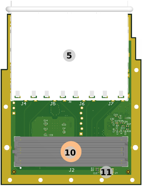
Figure 2: TEF0008-01 FMC overview.
...
On-board I2C devices are connected to the HPC FMC Pin C30 SCL and pin C31 SDA which are reserved for I2C. Level shift and for PLL and SFP+ I²C is done by the FPGA as well as MUX for SFP+. Addresses for on-board devices are listed in the table below:
| I2C Device | I2C Address | Notes |
|---|---|---|
| J4, SFP+ | ||
| J5, SFP+ | ||
| J6, SFP+ | ||
| J7, SFP+ | ||
| U2, Si5345A | 1101001 | Level shifted via MAX10 FPGA |
| U4, EEPROM | 10100xx | Last digits determined by carrier board via HPC FMC (C34 GA0, C35 GA1). |
Table 7: I2C slave device addresses.
...
There is a Silicon Labs I2C programmable quad PLL clock generator on-board (Si5338ASi5345A, U2) to generate various reference clocks for the module.
Not connected.
| Si5345A Pin |
|---|
| Signal Name / Description | Connected To | Direction | Note | |
|---|---|---|---|---|
IN0 | Reference input clock.- | U1 | Input | 25.000000 MHz oscillator, Si8208AI |
| IN1 | - | Not connected. | Input | Not used. |
IN2 | - |
IN4
| Not connected. | Input | Not used. |
IN3 |
Reference input clock.
| Input | |||
A1 |
- | GND | Input | I2C slave device address LSB |
IN5
-
| . |
| - | GND | Input | Not used. |
OUT0 |
CLK1_P
| U1, R23 | Output | FPGA bank 45. |
| OUT1 |
| - | U1, P23 | Output | FPGA bank 45. |
| OUT2 | U1, V5 | Output | FPGA MGT bank 225 reference clock. |
| OUT3 | - | U1, V6 | Output | FPGA MGT bank 225 reference clock. |
| OUT4 | - | U1, AB5 | Output | FPGA MGT bank 224 reference clock. |
| OUT5 | - | U1, AB6 | Output | FPGA MGT bank 224 reference clock. |
CLK0_P
| OUT6 | - | Output | FPGA bank 45. |
| OUT7 |
| GBTCLK0 | U1, pin T25 | Output | FPGA bank 45. | |
| OUT8 | CLK0 | |||
| OUT9 | CLK1 |
Table 8: Programmable quad PLL clock generator inputs and outputs.
...
Overview
Content Tools