Page History
...
| Scroll Title | ||||||||||||||||||||||||||||||
|---|---|---|---|---|---|---|---|---|---|---|---|---|---|---|---|---|---|---|---|---|---|---|---|---|---|---|---|---|---|---|
| ||||||||||||||||||||||||||||||
|
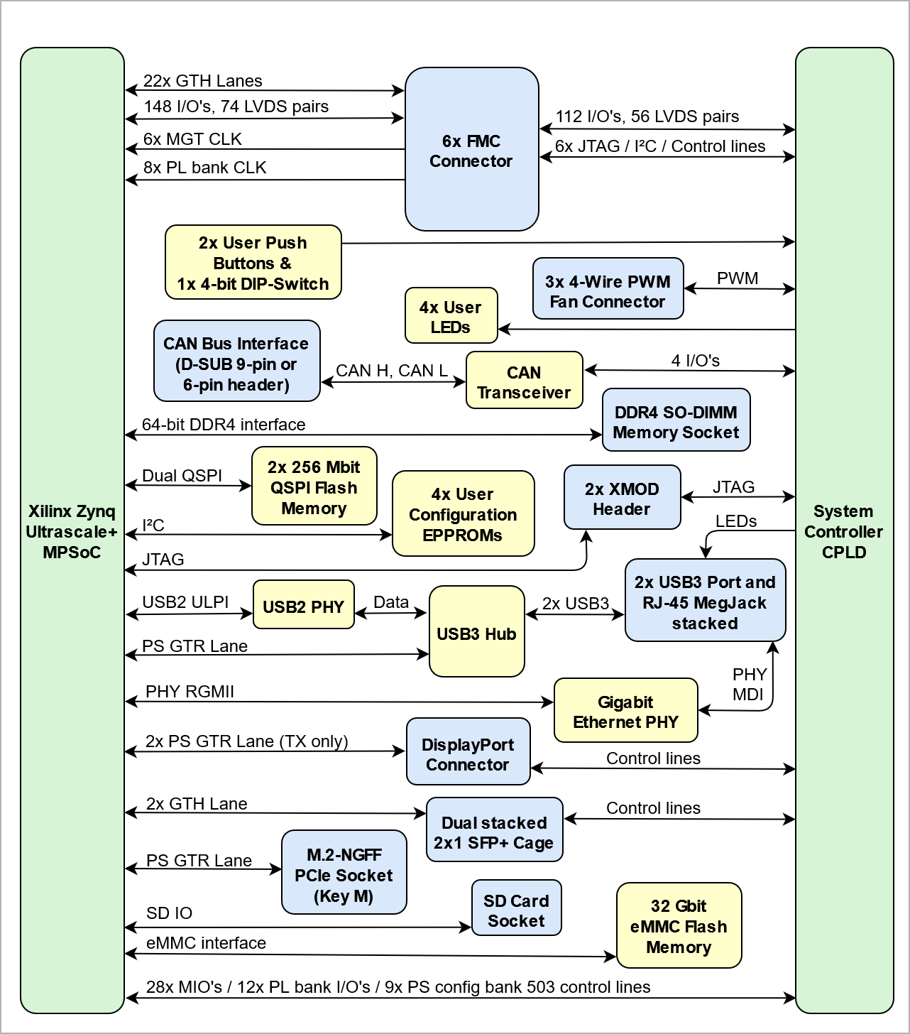
Main Components
| Scroll Title | ||||||||||||||||||||||||||||||
|---|---|---|---|---|---|---|---|---|---|---|---|---|---|---|---|---|---|---|---|---|---|---|---|---|---|---|---|---|---|---|
| ||||||||||||||||||||||||||||||
|
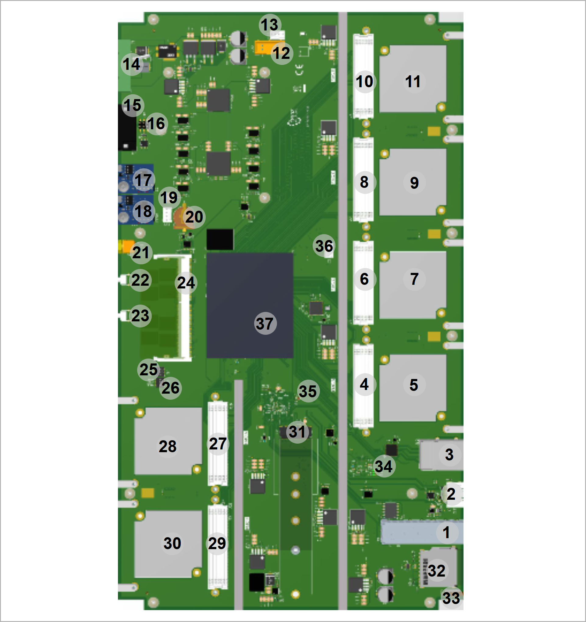
- SFP+ 2x1 cage with integrated LED light pipes, J9
- DisplayPort connector, J12
- USB3 A 2x , RJ45 1x (stacked), J13
- FMC connector (FMC B), J4
- FMC B cooling fan, M2
- FMC connector (FMC C), J8
- FMC C cooling fan, M3
- FMC connector (FMC D), J7
- FMC D cooling fan, M4
- FMC connector (FMC E), J6
- FMC E cooling fan, M5
- I²C programming header of on-board PLL clock generator U17, J22
- 4-Wire PWM fan connector, J23
- Main Power Jack 24V, J1
- CAN bus D-SUB 9-pin male connector, J3
- CAN bus 6-pin header male, J15
- XMOD JTAG header for access to System Controller CPLD, J35
- XMOD JTAG header for access to Zynq MPSoC, J24
- 4-Wire PWM fan connector, J33
- Battery Holder CR1220, B1
- SMA coaxial connector (PLL Si5345A U17 clock input), J25
- Push Button, S1
- Push Button, S2
- DDR4 SO-DIMM socket, U3
- 4-bit DIP-switch, S4
- 4-bit DIP-switch, S3
- FMC connector (FMC A), J10
- FMC A cooling fan, M1
- FMC connector (FMC F), J21
- FMC F cooling fan, M6
- NGFF M.2 PCIe socket (Key M), U2
- SD Card socket, J11
- User LEDs (3x green, 1x red) with LED light pipe, D13 ... D16
- Green LEDs dedicated to USB3 hub U4, D17 ... D19
- Red LED indicating FPGAs 'DONE' signal, D6
- 4-Wire PWM fan connector, J2
- Xilinx Zynq Ultrascale+ MPSoC, U1
Initial Delivery State
Storage device name | Content | Notes |
|---|---|---|
| User configuration EEPROMs (1x Microchip 24LC128-I/ST, 3x Microchip 24AA025E48T-I/OT) | Empty | Not programmed |
| USB3 HUB Configuration EEPROM (Microchip 24LC128-I/ST) | Empty | Not programmed |
| Si5338A programmable PLL NVM OTP | Empty | Not programmed |
| Si5345A programmable PLL NVM OTP | Empty | Not programmed |
| eMMC Flash memory | Empty | Not programmed |
| 2x QSPI Flash memory | Empty | Not programmed |
...
| HTML |
|---|
<!-- MGT lanes should be listed separately, as they are more specific than just general I/Os. --> |
Following tables contains information about the interfaces, I/O's, clock and VCCIO sources available on the FMC connectors A - F:
Anchor FMC A FMC A
FMC A
FMC A Interfaces:
| FMC | Interfaces | I/O Signal Count | LVDS-pairs count | Connected to | VCCO bank Voltage | Notes |
|---|---|---|---|---|---|---|
J10 (FMC A) | I/O | 12 | 6 | Bank 44 HD | FMCAF_1V8 | - |
| 56 | 28 | SC CPLD U27 Bank 1 | FMCAF_1V8 | - | ||
| I²C | 2 | - | I²C-Switch U37 | - | Muxed to MIO Bank 501 I²C Inteface | |
| JTAG | 4 | - | SC CPLD U27 Bank 2 | 3.3VSB | - | |
| MGT | - | 8 (4 x RX/TX) | Bank 128 GTH | - | 4x MGT lanes | |
| Clock Input | - | 1 | Bank 128 GTH | - | 1x Reference clock input to MGT bank | |
| Control Signals | 3 | - | SC CPLD U27 Bank 0 | 3.3VSB | 'FMCA_PG_C2M', 'FMCA_PG_M2C', 'FMCA_PRSNT' |
...
Table 7: FMC A connector cooling fan
Anchor FMC F FMC F
FMC F
FMC F Interfaces:
| FMC | Interfaces | I/O Signal Count | LVDS-pairs count | Connected to | VCCO bank Voltage | Notes |
|---|---|---|---|---|---|---|
J21 (FMC F) | I/O | 12 | 6 | Bank 44 HD | FMCAF_1V8 | - |
| 28 | 14 | SC CPLD U27 Bank 1 | FMCAF_1V8 | - | ||
| 28 | 14 | SC CPLD U27 Bank 3 | FMCAF_1V8 | - | ||
| I²C | 2 | - | I²C-Switch U37 | - | Muxed to MIO Bank 501 I²C Inteface | |
| JTAG | 4 | - | SC CPLD U27 Bank 2 | 3.3VSB | - | |
| MGT | - | 4 (2 x RX/TX) | Bank 129 GTH | - | 2x MGT lanes | |
| Clock Input | - | 1 | Bank 129 GTH | - | 1x Reference clock input to MGT bank | |
| Control Signals | 3 | - | SC CPLD U27 Bank 2 | 3.3VSB | 'FMCF_PG_C2M', 'FMCF_PG_M2C', 'FMCF_PRSNT' |
...
Table 12: FMC F connector cooling fan
Anchor FMC B FMC B
FMC B
FMC B Interfaces:
| FMC | Interfaces | I/O Signal Count | LVDS-pairs count | Connected to | VCCO bank Voltage | Notes |
|---|---|---|---|---|---|---|
J4 (FMC B) | I/O | 24 | 12 | Bank 47 HD | FMCBC_1V8 | - |
| 20 | 10 | Bank 48 HD | FMCBC_1V8 | - | ||
| 24 | 12 | Bank 49 HD | FMCBC_1V8 | - | ||
| I²C | 2 | - | I²C-Switch U13 | - | Muxed to MIO Bank 501 I²C Inteface | |
| JTAG | 4 | - | SC CPLD U27 Bank 0 | 3.3VSB | - | |
| MGT | - | 8 (4 x RX/TX) | Bank 130 GTH | - | 4x MGT lanes | |
| Clock Input | - | 2 | Bank 48 HD | - | 2x Reference clock inputs to PL bank | |
| - | 1 | Bank 130 GTH | - | 1x Reference clock input to MGT bank | ||
| Control Signals | 3 | - | SC CPLD U27 Bank 0 | 3.3VSB | 'FMCB_PG_C2M', 'FMCB_PG_M2C', 'FMCB_PRSNT' |
...
Table 17: FMC B connector cooling fan
Anchor FMC C FMC C
FMC C
FMC C Interfaces:
| FMC | Interfaces | I/O Signal Count | LVDS-pairs count | Connected to | VCCO bank Voltage | Notes |
|---|---|---|---|---|---|---|
J8 (FMC C) | I/O | 20 | 10 | Bank 50 HD | FMCBC_1V8 | - |
| 48 | 24 | Bank 67 HP | FMCBC_1V8 | - | ||
| I²C | 2 | - | I²C-Switch U13 | - | Muxed to MIO Bank 501 I²C Inteface | |
| JTAG | 4 | - | SC CPLD U27 Bank 2 | 3.3VSB | - | |
| MGT | - | 8 (4 x RX/TX) | Bank 230 GTH | - | 4x MGT lanes | |
| Clock Input | - | 2 | Bank 50 HD | - | 2x Reference clock inputs to PL bank | |
| - | 1 | Bank 230 GTH | - | 1x Reference clock input to MGT bank | ||
| Control Signals | 3 | - | SC CPLD U27 Bank 2 | 3.3VSB | 'FMCC_PG_C2M', 'FMCC_PG_M2C', 'FMCC_PRSNT' |
...
Table 22: FMC C connector cooling fan
Anchor FMC D FMC D
FMC D
FMC D Interfaces:
| FMC | Interfaces | I/O Signal Count | LVDS-pairs count | Connected to | VCCO bank Voltage | Notes |
|---|---|---|---|---|---|---|
J7 (FMC D) | I/O | 20 | 10 | Bank 65 HP | FMCDE_1V8 | - |
| 48 | 24 | Bank 66 HP | FMCDE_1V8 | - | ||
| I²C | 2 | - | I²C-Switch U13 | - | Muxed to MIO Bank 501 I²C Inteface | |
| JTAG | 4 | - | SC CPLD U27 Bank 2 | 3.3VSB | - | |
| MGT | - | 8 (4 x RX/TX) | Bank 229 GTH | - | 4x MGT lanes | |
| Clock Input | - | 2 | Bank 65 HP | - | 2x Reference clock inputs to PL bank | |
| - | 1 | Bank 229 GTH | - | 1x Reference clock input to MGT bank | ||
| Control Signals | 3 | - | SC CPLD U27 Bank 2 | 3.3VSB | 'FMCD_PG_C2M', 'FMCD_PG_M2C', 'FMCD_PRSNT' |
...
Table 27: FMC D connector cooling fan
Anchor FMC E FMC E
FMC E
FMC E Interfaces:
| FMC | Interfaces | I/O Signal Count | LVDS-pairs count | Connected to | VCCO bank Voltage | Notes |
|---|---|---|---|---|---|---|
J6 (FMC E) | I/O | 24 | 12 | Bank 65 HP | FMCDE_1V8 | - |
| 44 | 22 | Bank 64 HP | FMCDE_1V8 | - | ||
| I²C | 2 | - | I²C-Switch U13 | - | Muxed to MIO Bank 501 I²C Inteface | |
| JTAG | 4 | - | SC CPLD U27 Bank 2 | 3.3VSB | - | |
| MGT | - | 8 (4 x RX/TX) | Bank 228 GTH | - | 4x MGT lanes | |
| Clock Input | - | 2 | Bank 64 HP | - | 2x Reference clock inputs to PL bank | |
| - | 1 | Bank 228 GTH | - | 1x Reference clock input to MGT bank | ||
| Control Signals | 3 | - | SC CPLD U27 Bank 2 | 3.3VSB | 'FMCE_PG_C2M', 'FMCE_PG_M2C', 'FMCE_PRSNT' |
...
| Scroll Title | ||||||||||||||||||||||||||||||
|---|---|---|---|---|---|---|---|---|---|---|---|---|---|---|---|---|---|---|---|---|---|---|---|---|---|---|---|---|---|---|
| ||||||||||||||||||||||||||||||
|
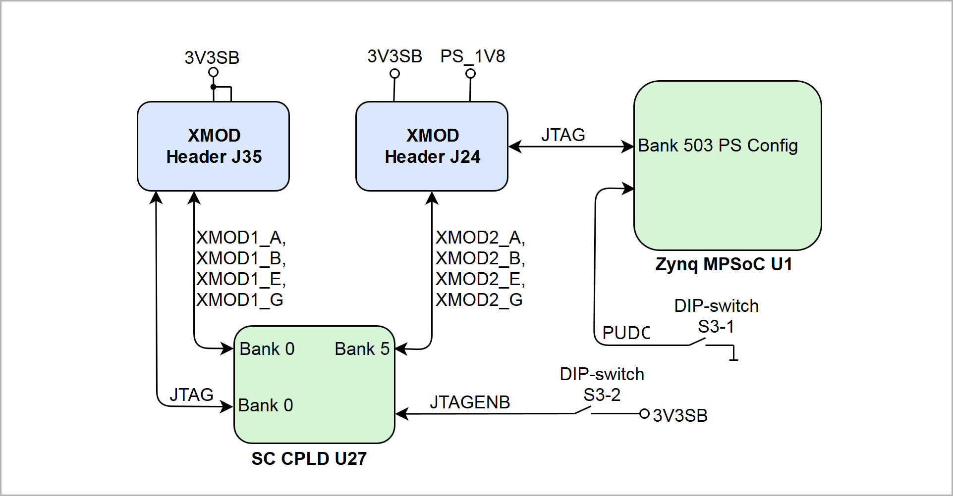
Signal Assignment of XMOD header J24 and J35
...
| Scroll Title | ||||||||||||||||||||||||||||||
|---|---|---|---|---|---|---|---|---|---|---|---|---|---|---|---|---|---|---|---|---|---|---|---|---|---|---|---|---|---|---|
| ||||||||||||||||||||||||||||||
|
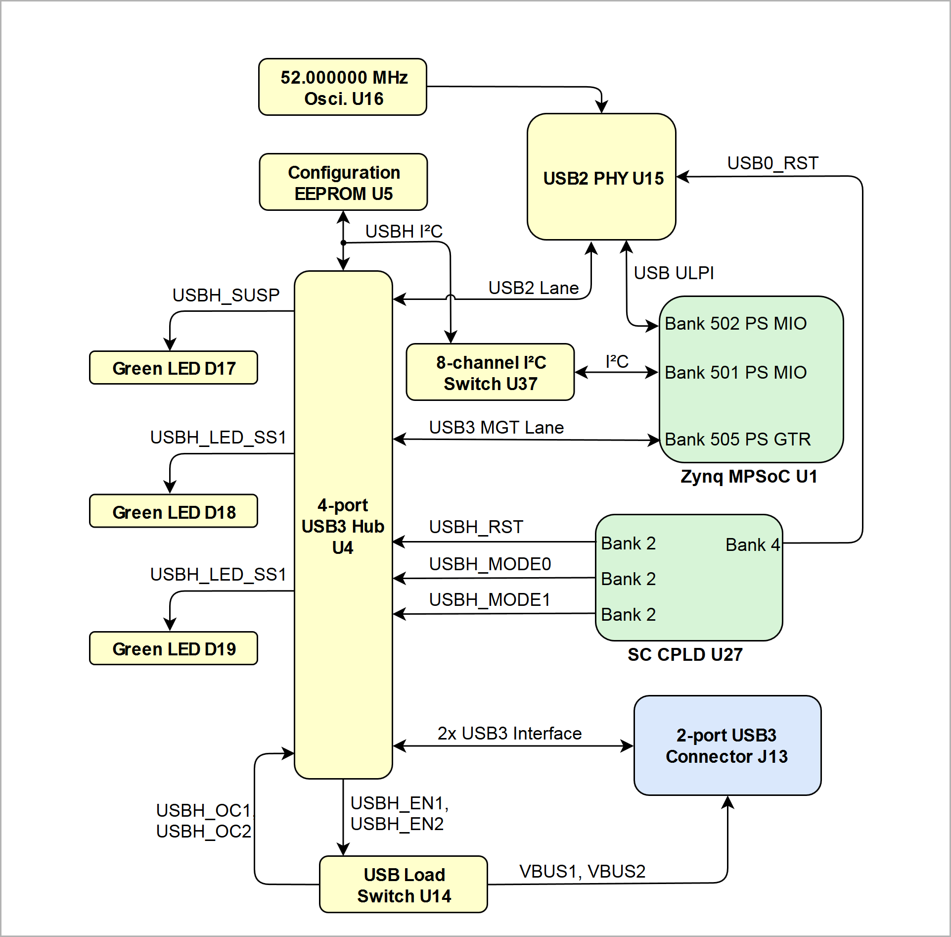
The 4-port USB3 hub is connected to the Zynq MPSoC's PS GTR bank, the USB2 PHY is connected to the PS MIO bank 502:
...
| Scroll Title | ||||||||||||||||||||||||||||||
|---|---|---|---|---|---|---|---|---|---|---|---|---|---|---|---|---|---|---|---|---|---|---|---|---|---|---|---|---|---|---|
| ||||||||||||||||||||||||||||||
|
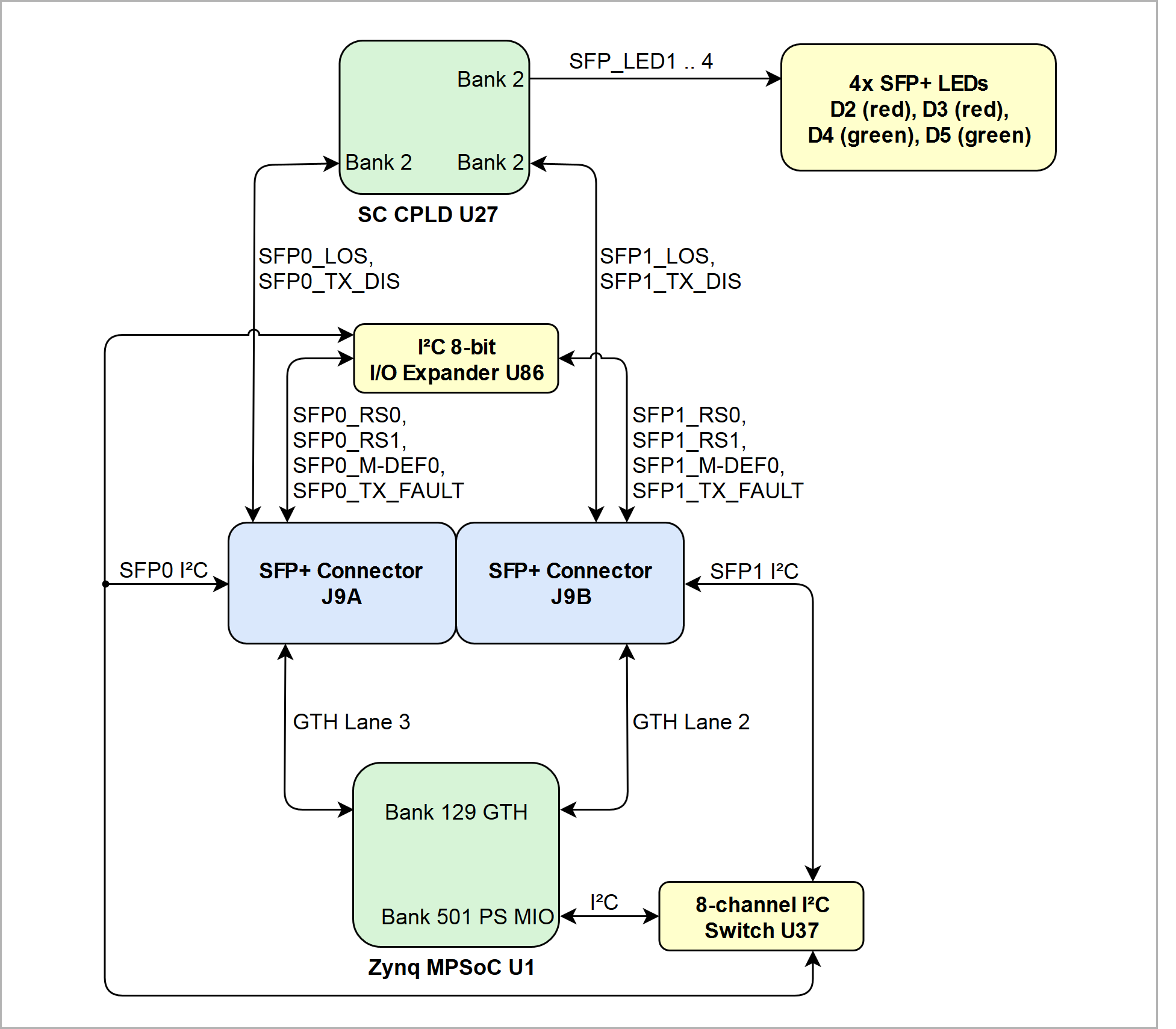
| Connector | Interface | Signal Schematic Name | Connected to | Logic | Notes |
|---|---|---|---|---|---|
SFP+ J9A | MGT Lane |
| MGTHTXP3_129, G31 | TX: Output RX: Input | Multi gigabit highspeed data lane |
| I²C |
| 8-channel I²C-switch U37 | BiDir | 2-wire Serial Interface | |
| Control Lines |
| I²C 8-bit I/O Port-Expander U86 | Output, low active | Full RX bandwidth | |
| Output, low active | Reduced RX bandwidth | |||
| Input, low active | Module present / not present | |||
| Input, high active | Fault / Normal Operation | |||
| SC CPLD U27, bank 2, pin V8 | Input, high active | Loss of receiver signal | ||
| SC CPLD U27, bank 2, pin Y7 | Output, low active | SFP Enabled / Disabled | ||
SFP+ J9B | MGT Lane |
| MGTHTXP2_129, H29 | TX: Output RX: Input | Multi gigabit highspeed |
| I²C |
| 8-channel I²C-switch U37 | Bidir | 2-wire Serial Interface | |
| Control Lines |
| I²C 8-bit I/O Port-Expander U86 | Output, low active | Full RX bandwidth | |
| Output, low active | Reduced RX bandwidth | |||
| Input, low active | Module present / not present | |||
| Input, high active | Fault / Normal Operation | |||
| SC CPLD U27, bank 2, pin W7 | Input, high active | Loss of receiver signal | ||
| SC CPLD U27, bank 2, pin V7 | Output. low active | SFP Enabled / Disabled |
...
| Scroll Title | ||||||||||||||||||||||||||||||
|---|---|---|---|---|---|---|---|---|---|---|---|---|---|---|---|---|---|---|---|---|---|---|---|---|---|---|---|---|---|---|
| ||||||||||||||||||||||||||||||
|

| Connector | Interface | Signal Schematic Name | Connected to | Notes |
|---|---|---|---|---|
M.2-NGFF PCIe Socket U2 | MGT Lane |
| PS_MGTRTXP0_505, AB29 | Multi gigabit highspeed TX: Output RX: Input |
| Clock Input |
| Quad programmable PLL clock generator U12, CLK0 | Reference clock signal | |
| Control Lines |
| SC CPLD U27, bank 2, pin AA13 | LED, Output, High active | |
| SC CPLD U27, bank 2, pin AA12 | PCIe sleep state, Input, Low active | ||
| SC CPLD U27, bank 2, pin AA11 | PCIe reset, Input, Low active | ||
| SC CPLD U27, bank 2, pin AB11 | PCIe Link reactivation, Input, Low active | ||
| connect to GND | PCIe Clock Request, Low active |
...
| Scroll Title | ||||||||||||||||||||||||||||||
|---|---|---|---|---|---|---|---|---|---|---|---|---|---|---|---|---|---|---|---|---|---|---|---|---|---|---|---|---|---|---|
| ||||||||||||||||||||||||||||||
|
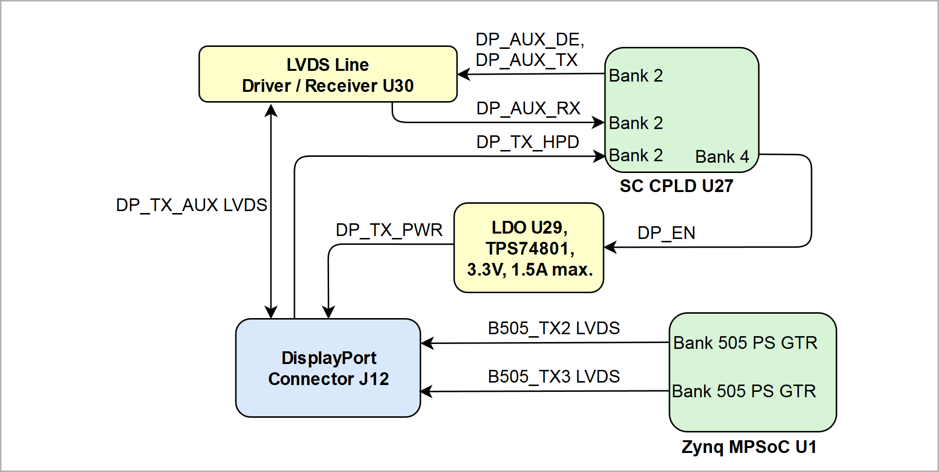
Follwowing table contains a brief description of the MGT lanes and control and status signals of the DisplayPort interface:
...
| Scroll Title | ||||||||||||||||||||||||||||||
|---|---|---|---|---|---|---|---|---|---|---|---|---|---|---|---|---|---|---|---|---|---|---|---|---|---|---|---|---|---|---|
| ||||||||||||||||||||||||||||||
|
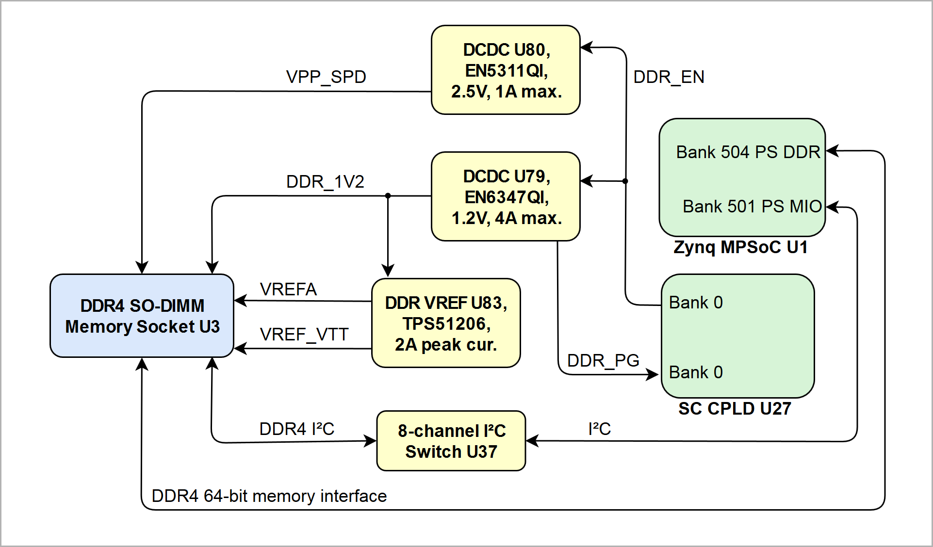
Following table gives an overview about the I/O signals of the DDR4 SDRAM memory interface:
...
| Scroll Title | ||||||||||||||||||||||||||||||
|---|---|---|---|---|---|---|---|---|---|---|---|---|---|---|---|---|---|---|---|---|---|---|---|---|---|---|---|---|---|---|
| ||||||||||||||||||||||||||||||
|
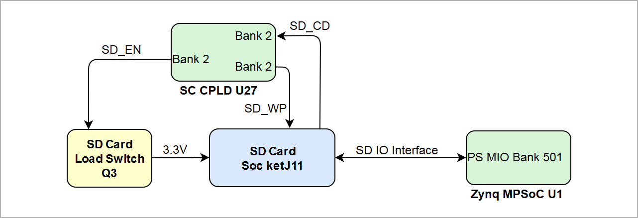
The SD Card socket have following signal and pin assignment:
...
| Scroll Title | ||||||||||||||||||||||||||||||
|---|---|---|---|---|---|---|---|---|---|---|---|---|---|---|---|---|---|---|---|---|---|---|---|---|---|---|---|---|---|---|
| ||||||||||||||||||||||||||||||
|
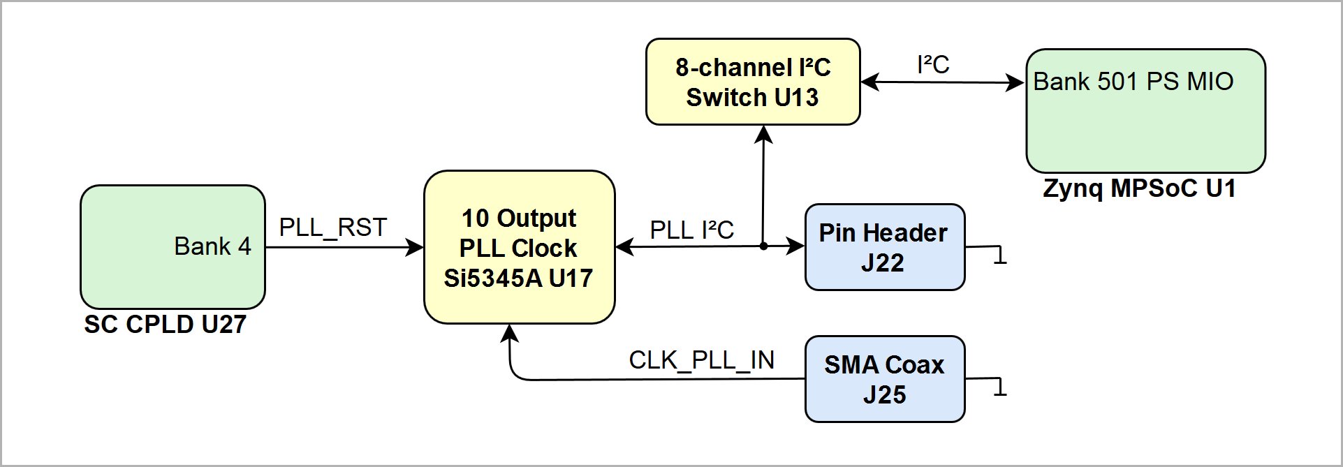
| Connector | Signal Schematic Name | Connected to | Notes |
|---|---|---|---|
Pin Header J22 |
| clock generator U17, pin 16 | PS_1V8 VCCIO |
| clock generator U17, pin 18 | ||
SMA Coax J25 |
| clock generator U17, pin 1 | - |
...
Table 65: Module hardware revision history
Hardware revision number can be found on the PCB board together with the board model number separated by the dash.
...
| HTML |
|---|
<!-- Generate new entry: 1.add new row below first 2.Copy "Page Information Macro(date)" Macro-Preview, Metadata Version number, Author Name and description to the empty row. Important Revision number must be the same as the Wiki document revision number 3.Update Metadata = "Page Information Macro (current-version)" Preview+1 and add Author and change description. --> |
Date | Revision | Contributors | Description | ||||||||||||||||||||||||||
|---|---|---|---|---|---|---|---|---|---|---|---|---|---|---|---|---|---|---|---|---|---|---|---|---|---|---|---|---|---|
|
|
|
| ||||||||||||||||||||||||||
| 2019-08-27 | v.184 | John Hartfiel |
| ||||||||||||||||||||||||||
| 2019-05-10 | v.183 | John Hartfiel |
| ||||||||||||||||||||||||||
| 2018-07-23 | v.182 | Ali Naseri |
| ||||||||||||||||||||||||||
| -- | all |
|
Table 66: Document change history
...
Overview
Content Tools