Page History
...
Storage device name | Content | Notes |
|---|---|---|
| User configuration EEPROMs (1x Microchip 24LC128-I/ST, 3x Microchip 24AA025E48T-I/OT) | Empty | Not programmed |
| USB3 .0 HUB Configuration EEPROM (Microchip 24LC128-I/ST) | Empty | Not programmed |
| Si5338A programmable PLL NVM OTP | Empty | Not programmed |
| Si5345A programmable PLL NVM OTP | Empty | Not programmed |
Table 1: Initial delivery state of programmable devices on the module.
...
Table 52: Programmable 10-output PLL clock generator inputs and outputsNote:
| Info |
|---|
The PLL clock generator U17 can be reseted by the low active pin 'PLL_RST' |
...
connected to SC CPLD U27, bank 4, pin L4 |
...
. |
On-board LEDs
The TEB0911 board is equipped with several LEDs to signal current states and activities.
...
Hence, those three power instances will be powered up consecutively and when the Power-Good -Signals signals of the previous instance is asserted.
...
| Scroll Title | ||||||||||||||||||||||||||
|---|---|---|---|---|---|---|---|---|---|---|---|---|---|---|---|---|---|---|---|---|---|---|---|---|---|---|
| ||||||||||||||||||||||||||
|
Power Rails
| Peripheral Designator | VCC / VCCIO Schematic Name | Voltage | Direction | Pins | Notes |
|---|---|---|---|---|---|
| J12 | DP_TX_PWR | 3.3V | Out | Pin 20 | Display-Port Connector |
| J9A | SFP_SSD | 3.3V | Out | Pin T15, T16 | SFP+ 2x1 Connector |
| J9B | SFP_SSD | 3.3V | Out | Pin L15, L16 | |
| J13A | VBUS1 | 5.0V | Out | Pin U1 | USB3 Ports |
| J13B | VBUS2 | 5.0V | Out | Pin U10 | |
| J11 | - | 3.3V | Out | Pin 4 | MicroSD Card Socket |
| B1 | PSBATT | 3.0V | In | Pin + | Battery Holder CR1220 |
| U2 | SSD1_3V3_1 | 3.3V | Out | Pin 2, 4 | SSD PCIe connector |
| SSD1_3V3_2 | 3.3V | Out | Pin 70, 72, 74 | ||
| SSD1_3V3_3 | 3.3V | Out | Pin 12, 14, 16, 18 | ||
| U3 | DDR_1V2 | 1.2V | Out | Pin 111, 112, 117, 118, 123, 124, 129, 130, 135, 136, 141, 142, 147, 148, 153, 154, 159, 160, 163 | DDR4 SO-DIMM socket |
| VPP_SPD | 2.5V | Out | Pin 255, 257, 259 |
Table 57: Power pin description of Peripherals' Connector
| XMOD / JTAG Designator | VCC / VCCIO Schematic Name | Voltage | Direction | Pins | Notes |
|---|---|---|---|---|---|
| J24 | 3V3SB | 3.3V | Out | Pin 5 | Zynq MPSoC JTAG |
| PS_1V8 | 1.8V | Out | Pin 6 | ||
| J35 | 3V3SB | 3.3V | Out | Pin 5, 6 | SC CPLD JTAG |
Table 58: Power pin description of XMOD/JTAG Connector
| Main Power | VCC / VCCIO Schematic Name | Voltage | Direction | Pins | Notes |
|---|---|---|---|---|---|
| J1 | PWR_IN_24V | 24V | In | Pin 2, 4 | 24V Power Jack |
Table 59: Power pin description of main power supply connector
| FMC Designator | VCC / VCCIO Schematic Name | Voltage | Direction | Pins | Notes |
|---|---|---|---|---|---|
| J10 | 12V_FMC_AF | 12.0V | Out | Pin C35, C37 | - |
| 3V3VSB | 3.3V | Out | Pin D32 | - | |
| FMCA_3V3 | 3.3V | Out | Pin D36, D38, D40, C39 | - | |
| FMCAF_1V8 | 1.8V | Out | Pin E39, G39, H40, F40 | - | |
| J21 | 12V_FMC_AF | 12.0V | Out | Pin C35, C37 | - |
| 3V3VSB | 3.3V | Out | Pin D32 | - | |
| FMCF_3V3 | 3.3V | Out | Pin D36, D38, D40, C39 | - | |
| FMCAF_1V8 | 1.8V | Out | Pin E39, G39, H40, F40 | - | |
| J4 | 12V | 12.0V | Out | Pin C35, C37 | - |
| 3V3VSB | 3.3V | Out | Pin D32 | - | |
| FMCB_3V3 | 3.3V | Out | Pin D36, D38, D40, C39 | - | |
| FMCBC_1V8 | 1.8V | Out | Pin E39, G39, H40, F40 | - | |
| J8 | 12V | 12.0V | Out | Pin C35, C37 | - |
| 3V3VSB | 3.3V | Out | Pin D32 | - | |
| FMCC_3V3 | 3.3V | Out | Pin D36, D38, D40, C39 | - | |
| FMCBC_1V8 | 1.8V | Out | Pin E39, G39, H40, F40 | - | |
| J7 | 12V | 12.0V | Out | Pin C35, C37 | - |
| 3V3VSB | 3.3V | Out | Pin D32 | - | |
| FMCD_3V3 | 3.3V | Out | Pin D36, D38, D40, C39 | - | |
| FMCDE_1V8 | 1.8V | Out | Pin E39, G39, H40, F40 | - | |
| J6 | 12V | 12.0V | Out | Pin C35, C37 | - |
| 3V3VSB | 3.3V | Out | Pin D32 | - | |
| FMCE_3V3 | 3.3V | Out | Pin D36, D38, D40, C39 | - | |
| FMCDE_1V8 | 1.8V | Out | Pin E39, G39, H40, F40 | - |
Table 60: Power pin description of FMC connectors
| FAN Designator | VCC / VCCIO Schematic Name | Voltage | Direction | Pins | Notes |
|---|---|---|---|---|---|
| J2 | - | 12.0V | Out | Pin 2 | headers for |
| optional cooling FANs | ||||
| J23 | - | 12.0V | Out | Pin 2 |
| J33 | - | 12.0V | Out | Pin 2 |
Table 61: Power pin description of FAN connectors
...
Variants Currently In Production
| Trenz shop TEB9011 overview page | |
|---|---|
| English page | German page |
Technical Specifications
Absolute Maximum Ratings
Parameter | Min | Max | Units | Reference Document |
|---|---|---|---|---|
VIN supply voltage | V | - | ||
Storage temperature | °C | - |
Table 63: Module absolute maximum ratings
...
| Parameter | Min | Max | Units | Reference Document |
|---|---|---|---|---|
| VIN supply voltage | ||||
| Operating temperature |
Table 64: Module recommended operating conditions
...
All dimensions are given in millimeters.
Put mechanical drawings here...
...
| Scroll Title | ||||
|---|---|---|---|---|
|
...
Revision History
Hardware Revision History
| Date | Revision | Notes | Link to PCN | Documentation Link |
|---|---|---|---|---|
| - | 03 | current available board revision | - | - |
| - | 02 | First production release | - | - |
| - | 01 | Prototypes | - | - |
Table 65: Module hardware revision history
...
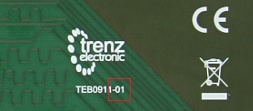
Hardware revision number can be found on the PCB board together with the module board model number separated by the dash.
Put picture of actual PCB showing model and hardware revision number here...
...
| Scroll Title | ||||
|---|---|---|---|---|
| ||||
|
Document Change History
| HTML |
|---|
<!-- Generate new entry: 1.add new row below first 2.Copy "Page Information Macro(date)" Macro-Preview, Metadata Version number, Author Name and description to the empty row. Important Revision number must be the same as the Wiki document revision number 3.Update Metadata = "Page Information Macro (current-version)" Preview+1 and add Author and change description. --> |
...
Date | Revision | Contributors | Description | ||||||||
|---|---|---|---|---|---|---|---|---|---|---|---|
| Ali Naseri | Initial document |
Table 66: Document change history
Disclaimer
| Include Page | ||||
|---|---|---|---|---|
|
NLVREF066
Overview
Content Tools