Page History
...
The Trenz Electronic TEB0911 UltraRack+ board is an industrial-grade motherboard integrating a Xilinx Zynq Ultrascale+ MPSoC with 4 GByte Flash memory for configuration and operation, DDR4-SDRAM SODIMM SO-DIMM socket with 64-bit wide data bus, 24 22 MGT Lanes lanes and powerful switch-mode power supplies for all on-board voltages.. The motherboard TEB0911 board exposes the pins of the Zynq MPSoC 's pins to accessible connectors and provides a whole range of on-board components to test and evaluate the Zynq Ultrascale+ MPSoC and for developing purposes. The motherboard board is capable to be fitted to a dedicated enclosure. On , whereby on the enclosure's rear and front panel, I/O's, LVDS-pairs and MGT interfaces lanes are accessible through 6 on-board FMC connectors and other standard high-speed interfaces for , namely USB3.0, SFP+, SSD, GbE, etc.
Key Features
- Single 24V main power supply
- 2x USB3 A Connector (Superspeed Host Port (Highspeed in USB2 mode))
- Gigabit Ethernet RGMII PHY with RJ45 MegJack
- Dual SFP+ Connector (2x1 Cage)
- DDR4-SDRAM SODIMM SO-DIMM socket (64bit bus width)
- SSD (Solid State Disk) ConnectorPCIe connector
- CAN FD Transceiver (10 Pin IDC interface (D-SUB 9-pin male connector and 6-pin header)
- 1x DisplayPort (2 lanes)
- 4x On-board configuration EEPROMs (1x Microchip 24LC128-I/ST, 3x Microchip 24AA025E48T-I/OT)
- All carrier board peripherals' I²C interfaces muxed to MPSoC's I²C interface
- 6x FMC HPC Connectorsconnectors
- 6x FMC Fans
- 3x Optional 3x 4-wire PWM fan connectors
- 10 output programmable PLL clock generator Si5345A
- Quad programmable PLL clock generator SI5338A
- 1x SMA coaxial connectors for reference clock signal input
- MicroSD-Socket SD Card socket (bootable)
- 32 Gbit (4 GByte) on-board eMMC flash (8 banks a 4 Gbit)
- System Controller CPLD Lattice MachXO2 7000 HC
- 2x JTAG/UART header ('XMOD FTDI JTAG Adapter'-compatible) XMOD header for programming MPSoC and SC CPLD
- On-board DC-DC PowerSoCs and LDOs
...
| Scroll Title | ||||||||||||||||||||||||||
|---|---|---|---|---|---|---|---|---|---|---|---|---|---|---|---|---|---|---|---|---|---|---|---|---|---|---|
| ||||||||||||||||||||||||||
|
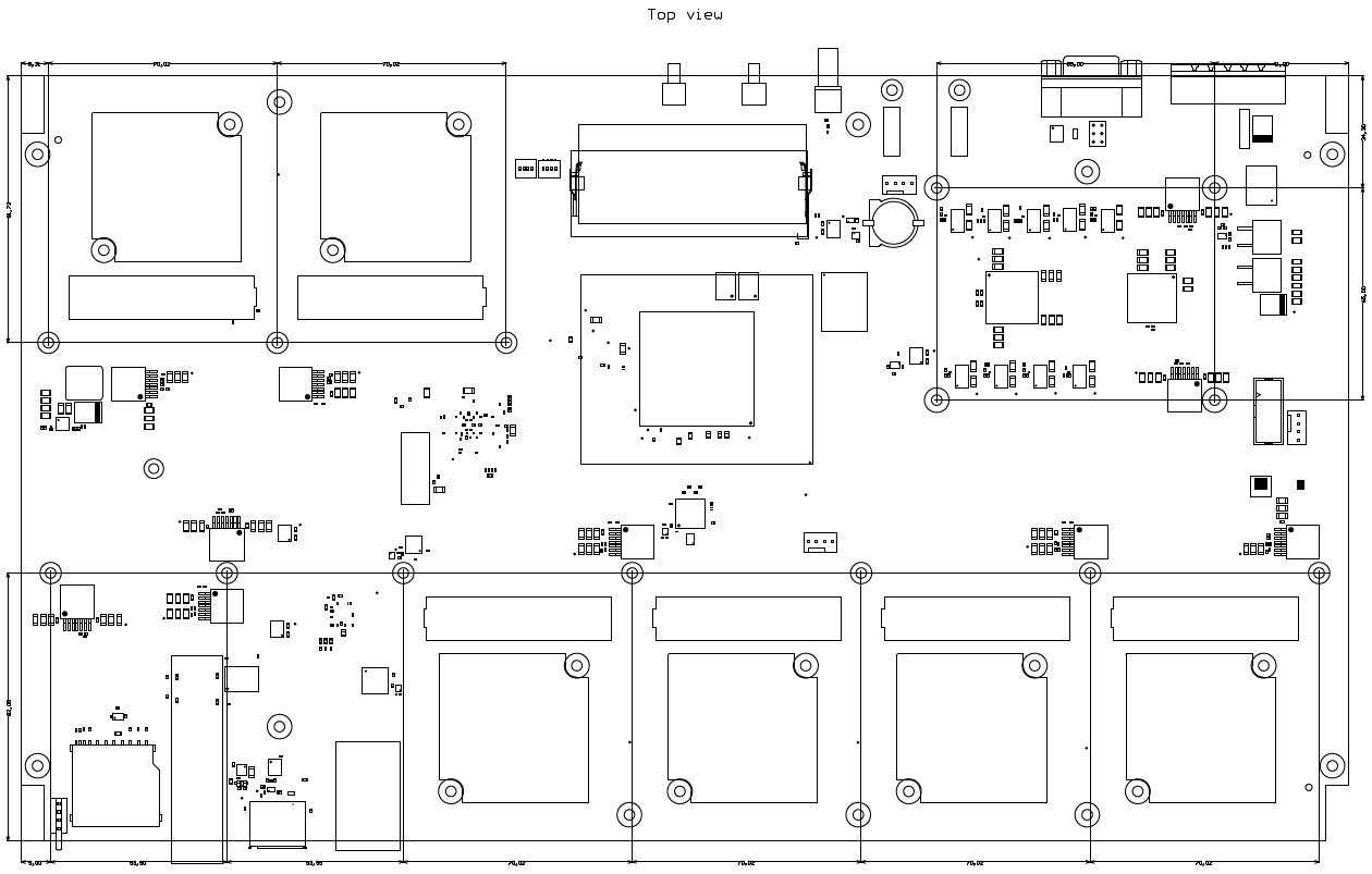
Main Components
| Scroll Title | ||||||||||||||||||||||||||
|---|---|---|---|---|---|---|---|---|---|---|---|---|---|---|---|---|---|---|---|---|---|---|---|---|---|---|
| ||||||||||||||||||||||||||
|
- SFP+ 2x1 cage with integrated LED light pipes, J9
- DisplayPort connector, J12
- USB3 A 2x , RJ45 1x (stacked), J13
- FMC connector (FMC B), J4
- FMC B cooling fan, M2
- FMC connector (FMC C), J8
- FMC C cooling fan, M3
- FMC connector (FMC D), J7
- FMC D cooling fan, M4
- FMC connector (FMC E), J6
- FMC E cooling fan, M5
- I²C programming header of on-board PLL clock generator U17, J22
- 4-Wire PWM fan connector, J23
- Main Power Jack 24V, J1
- CAN bus D-SUB 9-pin male connector, J3
- CAN bus 6-pin header male, J15
- XMOD JTAG header for access to System Controller CPLD, J35
- XMOD JTAG header for access to Zynq MPSoC, J24
- 4-Wire PWM fan connector, J33
- Battery Holder CR1220, B1
- SMT coaxial connector (PLL Si5345A U17 clock input), J25
- Push Button, S1
- Push Button, S2
- DDR4 SO-DIMM socket, U3
- 4-bit DIP-switch, S4
- 4-bit DIP-switch, S3
- FMC connector (FMC A), J10
- FMC A cooling fan, M1
- FMC connector (FMC F), J21
- FMC F cooling fan, M6
- NGFF M.2 PCIe socket (Key M), U2
- SD Card socket, J11
- User LEDs (3x green, 1x red) with LED light pipe, D13 ... D16
- Green LEDs dedicated to USB3 hub U4, D17 ... D19
- Red LED indicating FPGAs 'DONE' signal, D6
- 4-Wire PWM fan connector, J2
- Xilinx Zynq Ultrascale+ MPSoC, U1
...
Storage device name | Content | Notes |
|---|---|---|
| User configuration EEPROMs (1x Microchip 24LC128-I/ST, 3x Microchip 24AA025E48T-I/OT) | Empty | Not programmed |
| USB3 HUB Configuration EEPROM (Microchip 24LC128-I/ST) | Empty | Not programmed |
| Si5338A programmable PLL NVM OTP | Empty | Not programmed |
| Si5345A programmable PLL NVM OTP | Empty | Not programmed |
| eMMC Flash memory | Empty | Not programmed |
| 2 QSPI Flash memory | Empty | Not programmed |
Table 1: Initial delivery state of programmable devices on the module.
...
| Scroll Title | ||||||||||||||||||||||||||
|---|---|---|---|---|---|---|---|---|---|---|---|---|---|---|---|---|---|---|---|---|---|---|---|---|---|---|
| ||||||||||||||||||||||||||
|
| HTML |
|---|
<!-- MGT lanes should be listed separately, as they are more specific than just general I/Os. --> |
...
| Scroll Title | ||||||||||||||||||||
|---|---|---|---|---|---|---|---|---|---|---|---|---|---|---|---|---|---|---|---|---|
| ||||||||||||||||||||
|
| Connector | Interface | Signal Schematic Name | Connected to | Logic | Notes |
|---|---|---|---|---|---|
SFP+ J9A | MGT Lane |
| MGTHTXP3_129, G31 | TX: Output RX: Input | Multi gigabit highspeed data lane |
| I²C |
| 8-channel I²C-switch U37 | BiDir | 2-wire Serial Interface | |
| Control Lines |
| I²C 8-bit I/O Port-Expander U86 | Output, low active | Full RX bandwidth | |
| Output, low active | Reduced RX bandwidth | |||
| Input, low active | Module present / not present | |||
| Input, high active | Fault / Normal Operation | |||
| SC CPLD U27, bank 2, pin V8 | Input, high active | Loss of receiver signal | ||
| SC CPLD U27, bank 2, pin Y7 | Output, low active | SFP Enabled / Disabled | ||
SFP+ J9B | MGT Lane |
| MGTHTXP2_129, H29 | TX: Output RX: Input | Multi gigabit highspeed |
| I²C |
| 8-channel I²C-switch U37 | Bidir | 2-wire Serial Interface | |
| Control Lines |
| I²C 8-bit I/O Port-Expander U86 | Output, low active | Full RX bandwidth | |
| Output, low active | Reduced RX bandwidth | |||
| Input, low active | Module present / not present | |||
| Input, high active | Fault / Normal Operation | |||
| SC CPLD U27, bank 2, pin W7 | Input, high active | Loss of receiver signal | ||
| SC CPLD U27, bank 2, pin V7 | Output. low active | SFP Enabled / Disabled |
...
| Scroll Title | ||||||||||||||||||||||||
|---|---|---|---|---|---|---|---|---|---|---|---|---|---|---|---|---|---|---|---|---|---|---|---|---|
| ||||||||||||||||||||||||
|
Power distribution to the MPSoC PS and PL units:
...
The TEB0911 board is capable to be operated at an operational temperatur range of 0 °C ... 85 °C without FMC cooling fans M1 ... M6 and NGFF M.2 PCIe socket U2.
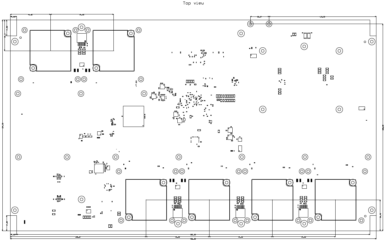
Physical Dimensions
Module Board size: ... mm 406mm × 234... mm30mm. Please download the assembly diagram for exact numbers.Mating height with standard connectors: ... mm.
PCB thickness: 1... 65 mm.
Highest part on PCB: approx. ... mm. Please download the step model for exact numbers.
...
| Scroll Title | ||||
|---|---|---|---|---|
| ||||
|
| Scroll Title | ||||
|---|---|---|---|---|
| ||||
|
Revision History
Hardware Revision History
...
| Include Page | ||||
|---|---|---|---|---|
|
...
Overview
Content Tools