Page History
| Scroll Ignore |
|---|
Download PDF version of this document. |
| Scroll pdf ignore | |
|---|---|
Table of Contents
|
...
Figure 2: 4 x 5 SoM carrier board TE0705-04.
- ARM JTAG Connector (DS-5 D-Stream) J15 - PJTAG to EMIO multiplexing needed
- 12-pin IDC header socket J1 (right angle, max. VCCIO voltage 3.3V)
RJ45 GbE Connector
- SD Card Socket - Zynq SDIO0 bootable SD port
- 12-pin IDC header socket (right angle) J2
- Micro USB Connector J12 (Device, Host or OTG Modes)
- Battery holder for CR1220 (RTC backup voltage)
- 12-pin IDC header socket (vertical) J5
- 12-pin IDC header socket (vertical) J6
- User Push-Button S2 ("RESTART" button by default)
- User Push-Button S1 ("RESET" button by default)
- User LEDs D6, D7, D8, D9
- User LEDs D4, D5, D14, D15
- Mini USB Connector (USB JTAG and UART Interface) J7
- User 4-bit DIP-Switch S3
- User 4-bit DIP-Switch S4
- FTDI FT2232H USB 2.0 High Speed to UART/FIFO
- Lattice Semiconductor MachXO2 1200HC System Controller CPLD
- Jumper J4 to fix user button S2 to switched state
- 40-Pin-Header J13 for access to PL IO-bank-pins
- 40-Pin-Header J11 for access to PL IO-bank-pins
- Samtec Razor Beam™ LSHM-150 B2B connector JB1
- Samtec Razor Beam™ LSHM-150 B2B connector JB2
- Samtec Razor Beam™ LSHM-130 B2B connector JB3
- Barrel jack for 12V power supply J10
- Jumper J21 to select supply voltage of VIOTB
- Jumper J9, J19, J20 to select supply voltage of USB-VBUS
...
The PL IO-bank supply voltage FMC_VADJ is available after the output of the 5.0V DC-DC converter is active and the EN_FMC pin of the System Controller CPLD is asserted.
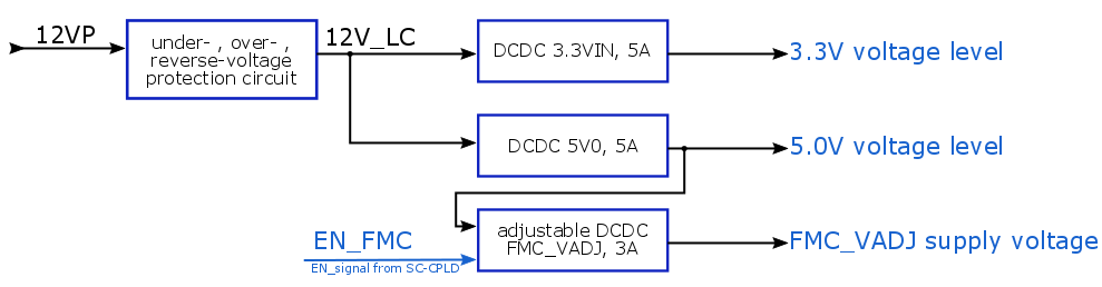
Figure 3: Power-On sequence diagram.
...
With jumper J21, user can select between two different power sources for SoM PL IO banks supply voltage VIOTB. If set to position 1-2, fixed 3.3V is selected as VIOTB source. If set to position 2-3, FMC_VADJ is selected as VIOTB source. Voltage level of FMC_VADJ depends on the settings of DIP-switch S3, see table below:
| J21 Position | S3-1 (CM1) | S3-2 (CM0) | FMC_VADJ Voltage | VIOTB Voltage | Notes | |
|---|---|---|---|---|---|---|
| 1-2 | - | - | - | 3.3V | ||
| 2-3 | OFF | OFF | 1.8V | 1.8V | ||
| 2-3 | OFF | ON | 2.5V | 2.5V | ||
| 2-3 | ON | OFF | 3.3V | 3.3V | ||
| 2-3 | ON | ON | 1.8V | 1.8V | This setting also enables JTAG access to the System Controller CPLD on the SoM via B2B connector JB2. |
Table 3: Jumper J21 and DIP-switch S3 settings for VIOTB voltage configuration.
Note: Exact function of the S3-1 and S3-2 switches depend on the TE0705 System Controller CPLD firmware. For more detailed information, refer to the documentation of the TE0705 System Controller CPLD.
...
| Date | Revision | Notes | PCN | Documentation link |
|---|---|---|---|---|
| 2016-10-04 | 04 | - | - | TE0705-04 |
Figure 5: Hardware revision number.
...
Overview
Content Tools