...
| Scroll Title |
|---|
| anchor | Figure_1 |
|---|
| title | Figure 1: TEB0911-03 block diagram |
|---|
|
| Scroll Ignore |
|---|
| draw.io Diagram |
|---|
| border | false |
|---|
| viewerToolbar | true |
|---|
| |
|---|
| fitWindow | false |
|---|
| diagramName | TEB0911 block diagram |
|---|
| simpleViewer | false |
|---|
| width | |
|---|
| links | auto |
|---|
| tbstyle | hidden |
|---|
| lbox | true |
|---|
| diagramWidth | 641 |
|---|
| revision |
|---|
|
|
11| Scroll Only |
|---|
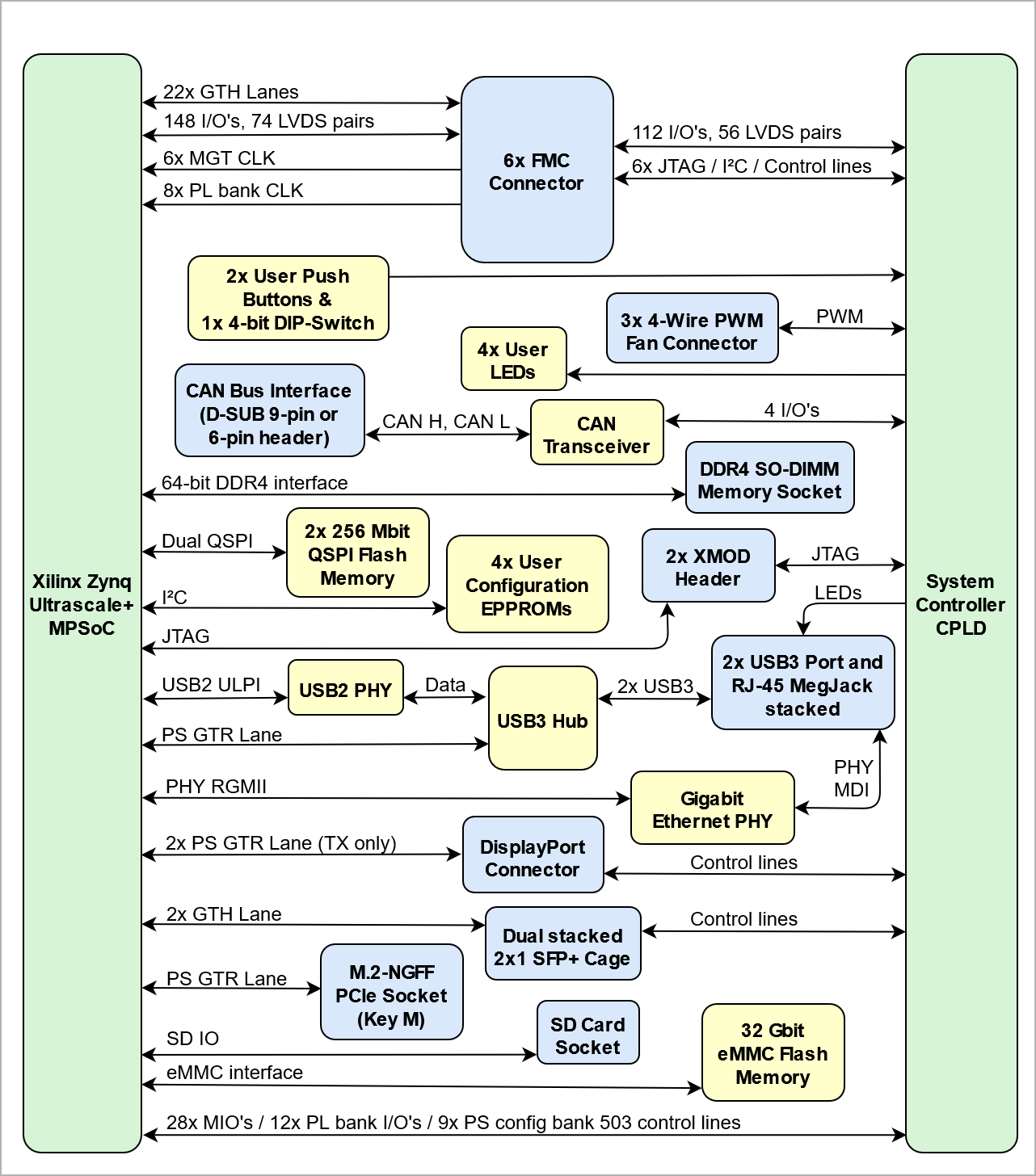 Image Added Image Added
|
|
Main Components
| Scroll Title |
|---|
| anchor | Figure_2 |
|---|
| title | Figure 2: TEB0911-03 main components |
|---|
|
| Scroll Ignore |
|---|
| draw.io Diagram |
|---|
| border | false |
|---|
| viewerToolbar | true |
|---|
| |
|---|
| fitWindow | false |
|---|
| diagramName | TEB0911-03 main components |
|---|
| simpleViewer | false |
|---|
| width | |
|---|
| links | auto |
|---|
| tbstyle | hidden |
|---|
| lbox | true |
|---|
| diagramWidth | 641 |
|---|
| revision | 8 |
|---|
|
|
| Scroll Only |
|---|
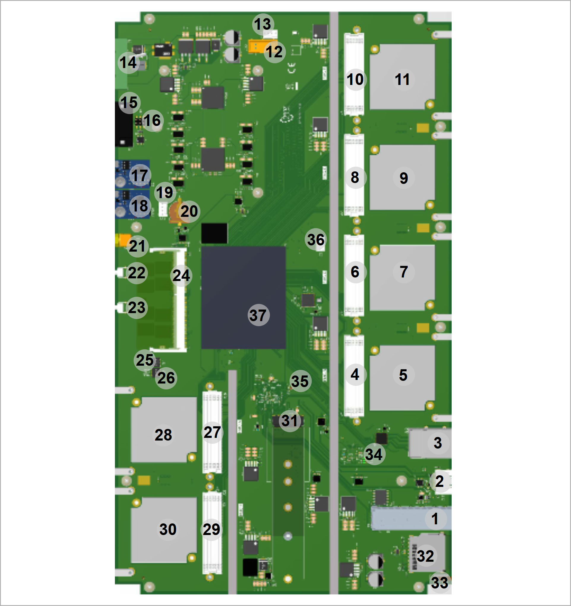 Image Added Image Added
|
|
- SFP+ 2x1 cage with integrated LED light pipes, J9
- DisplayPort connector, J12
- USB3 A 2x , RJ45 1x (stacked), J13
- FMC connector (FMC B), J4
- FMC B cooling fan, M2
- FMC connector (FMC C), J8
- FMC C cooling fan, M3
- FMC connector (FMC D), J7
- FMC D cooling fan, M4
- FMC connector (FMC E), J6
- FMC E cooling fan, M5
- I²C programming header of on-board PLL clock generator U17, J22
- 4-Wire PWM fan connector, J23
- Main Power Jack 24V, J1
- CAN bus D-SUB 9-pin male connector, J3
- CAN bus 6-pin header male, J15
- XMOD JTAG header for access to System Controller CPLD, J35
- XMOD JTAG header for access to Zynq MPSoC, J24
- 4-Wire PWM fan connector, J33
- Battery Holder CR1220, B1
- SMA coaxial connector (PLL Si5345A U17 clock input), J25
- Push Button, S1
- Push Button, S2
- DDR4 SO-DIMM socket, U3
- 4-bit DIP-switch, S4
- 4-bit DIP-switch, S3
- FMC connector (FMC A), J10
- FMC A cooling fan, M1
- FMC connector (FMC F), J21
- FMC F cooling fan, M6
- NGFF M.2 PCIe socket (Key M), U2
- SD Card socket, J11
- User LEDs (3x green, 1x red) with LED light pipe, D13 ... D16
- Green LEDs dedicated to USB3 hub U4, D17 ... D19
- Red LED indicating FPGAs 'DONE' signal, D6
- 4-Wire PWM fan connector, J2
- Xilinx Zynq Ultrascale+ MPSoC, U1
...
| Scroll Title |
|---|
| anchor | Figure_3 |
|---|
| title | Figure 3: General overview of the FMC connectors |
|---|
|
| Scroll Ignore |
|---|
| draw.io Diagram |
|---|
| border | false |
|---|
| viewerToolbar | true |
|---|
| |
|---|
| fitWindow | false |
|---|
| diagramName | FMC Diagramm formatted |
|---|
| simpleViewer | false |
|---|
| width | |
|---|
| links | auto |
|---|
| tbstyle | hidden |
|---|
| lbox | true |
|---|
| diagramWidth | 641 |
|---|
| revision |
|---|
|
|
7| Scroll Only |
|---|
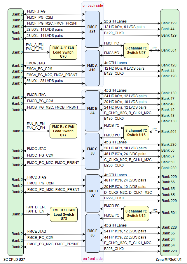 Image Added Image Added
|
|
| HTML |
|---|
<!--
MGT lanes should be listed separately, as they are more specific than just general I/Os.
--> |
...
| Scroll Title |
|---|
| anchor | Figure_4 |
|---|
| title | Figure 4: XMOD header J24 and J35 |
|---|
|
| Scroll Ignore |
|---|
| draw.io Diagram |
|---|
| border | false |
|---|
| viewerToolbar | true |
|---|
| |
|---|
| fitWindow | false |
|---|
| diagramName | XMOD header diagram formatted |
|---|
| simpleViewer | false |
|---|
| width | |
|---|
| links | auto |
|---|
| tbstyle | hidden |
|---|
| lbox | true |
|---|
| diagramWidth | 641 |
|---|
| revision | 1 |
|---|
|
|
| Scroll Only |
|---|
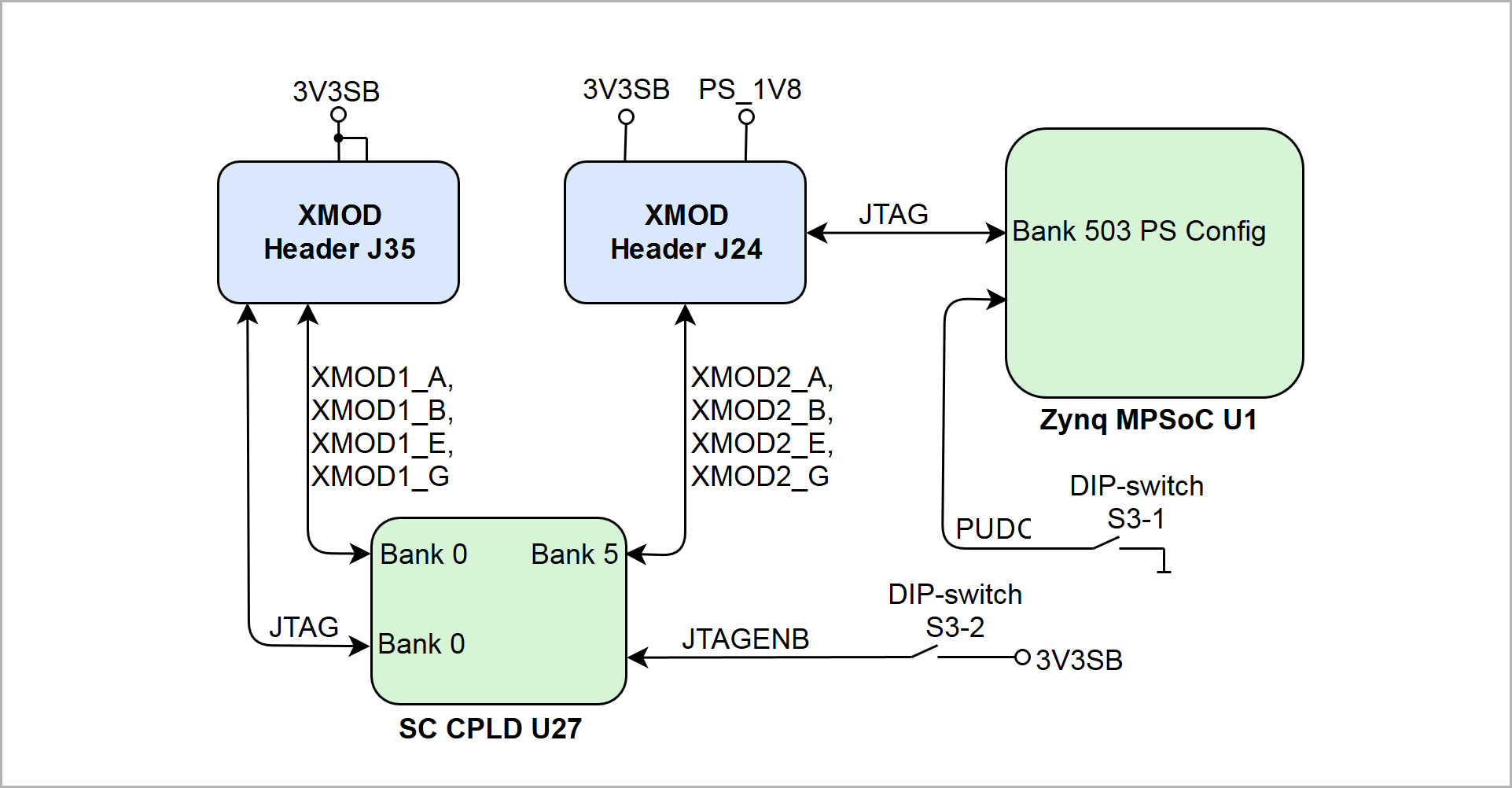 Image Added Image Added
|
|
Signal Assignment of XMOD header J24 and J35
...
| Scroll Title |
|---|
| anchor | Figure_5 |
|---|
| title | Figure 5: Gigabit Ethernet interface |
|---|
|
| Scroll Ignore |
|---|
| draw.io Diagram |
|---|
| border | false |
|---|
| viewerToolbar | true |
|---|
| |
|---|
| fitWindow | false |
|---|
| diagramName | Gigabit Ethernet interface diagram formatted |
|---|
| simpleViewer | false |
|---|
| width | |
|---|
| links | auto |
|---|
| tbstyle | hidden |
|---|
| lbox | true |
|---|
| diagramWidth | 641 |
|---|
| revision | 2 |
|---|
|
|
| Scroll Only |
|---|
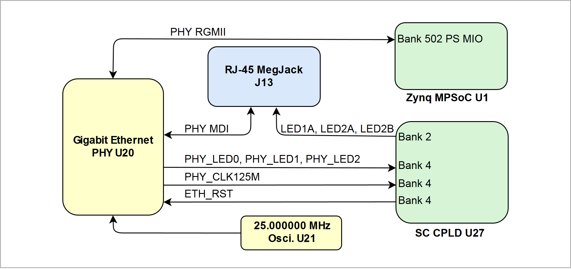 Image Added Image Added
|
|
Following table describes the signals and control lines of the Gigabit Ethernet interface of the board:
...
| Scroll Title |
|---|
| anchor | Figure_6 |
|---|
| title | Figure 6: USB3 interface |
|---|
|
| Scroll Ignore |
|---|
| draw.io Diagram |
|---|
| border | false |
|---|
| viewerToolbar | true |
|---|
| |
|---|
| fitWindow | false |
|---|
| diagramName | USB3 interface diagram formatted |
|---|
| simpleViewer | false |
|---|
| width | |
|---|
| links | auto |
|---|
| tbstyle | hidden |
|---|
| lbox | true |
|---|
| diagramWidth | 641 |
|---|
| revision | 1 |
|---|
|
|
| Scroll Only |
|---|
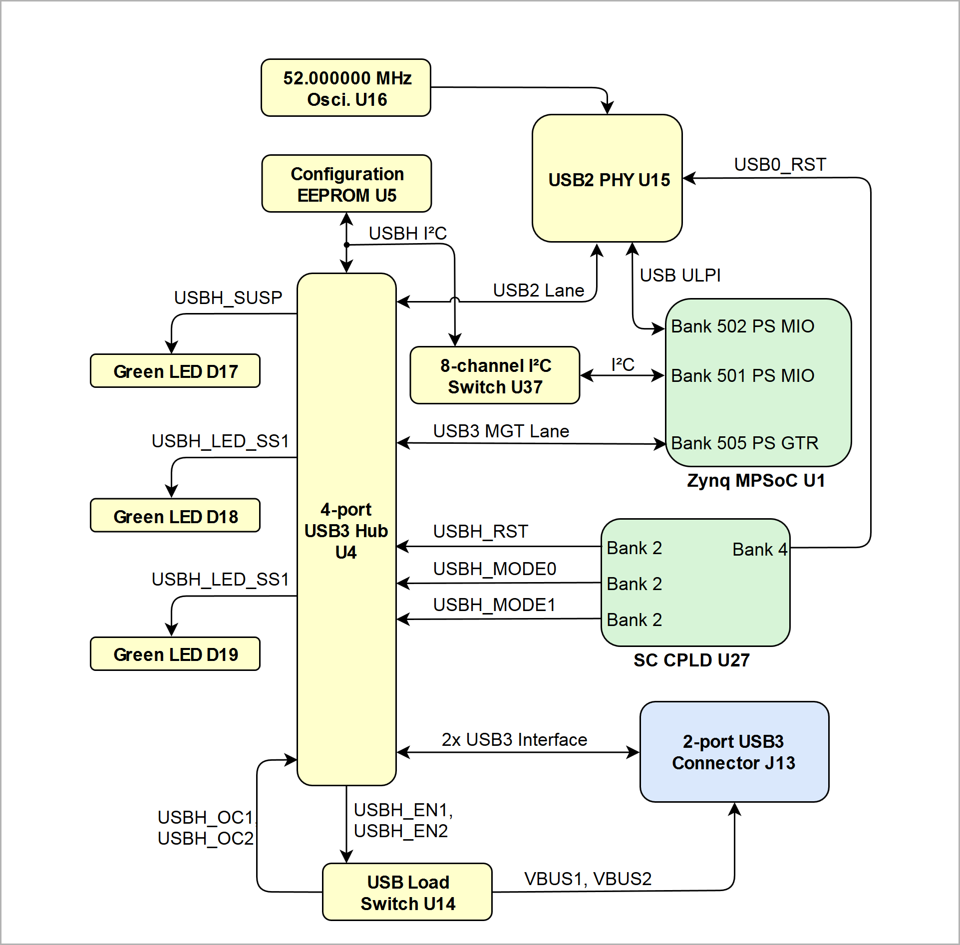 Image Added Image Added
|
|
The 4-port USB3 hub is connected to the Zynq MPSoC's PS GTR bank, the USB2 PHY is connected to the PS MIO bank 502:
...
| Scroll Title |
|---|
| anchor | Figure_7 |
|---|
| title | Figure 7: SFP+ interface |
|---|
|
| Scroll Ignore |
|---|
| draw.io Diagram |
|---|
| border | false |
|---|
| viewerToolbar | true |
|---|
| |
|---|
| fitWindow | false |
|---|
| diagramName | SFP interface diagram formatted |
|---|
| simpleViewer | false |
|---|
| width | |
|---|
| links | auto |
|---|
| tbstyle | hidden |
|---|
| lbox | true |
|---|
| diagramWidth | 641 |
|---|
| revision | 2 |
|---|
|
|
| Scroll Only |
|---|
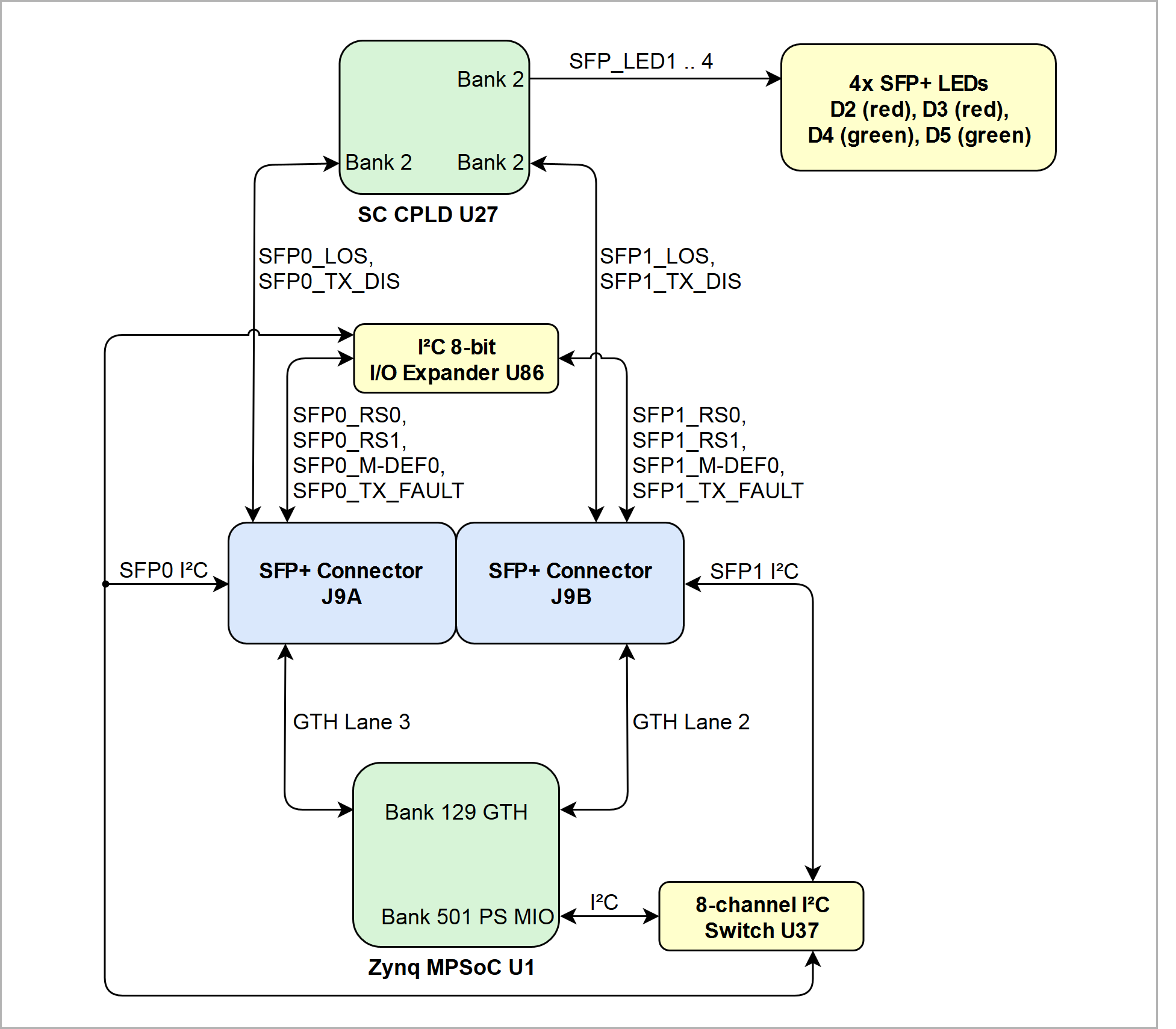 Image Added Image Added
|
|
| Connector | Interface | Signal Schematic Name | Connected to | Logic | Notes |
|---|
SFP+ J9A | MGT Lane | - B129_TX3_P
- B129_TX3_N
- B129_RX3_P
- B129_RX3_N
| MGTHTXP3_129, G31
MGTHTXN3_129, G32
MGTHRXP3_129, F33
MGTHRXN3_129, F34 | TX: Output RX: Input | Multi gigabit highspeed
data lane |
| I²C | | 8-channel I²C-switch U37 | BiDir | 2-wire Serial Interface |
| Control Lines | | I²C 8-bit I/O Port-Expander U86 | Output, low active | Full RX bandwidth |
| Output, low active | Reduced RX bandwidth |
| Input, low active | Module present / not present |
| Input, high active | Fault / Normal Operation |
| SC CPLD U27, bank 2, pin V8 | Input, high active | Loss of receiver signal |
| SC CPLD U27, bank 2, pin Y7 | Output, low active | SFP Enabled / Disabled |
SFP+ J9B | MGT Lane | - B129_TX2_P
- B129_TX2_N
- B129_RX2_P
- B129_RX2_N
| MGTHTXP2_129, H29
MGTHTXN2_129, H30
MGTHRXP2_129, H33
MGTHRXN2_129, H34 | TX: Output RX: Input | Multi gigabit highspeed
data lane |
| I²C | | 8-channel I²C-switch U37 | Bidir | 2-wire Serial Interface |
| Control Lines | | I²C 8-bit I/O Port-Expander U86 | Output, low active | Full RX bandwidth |
| Output, low active | Reduced RX bandwidth |
| Input, low active | Module present / not present |
| Input, high active | Fault / Normal Operation |
| SC CPLD U27, bank 2, pin W7 | Input, high active | Loss of receiver signal |
| SC CPLD U27, bank 2, pin V7 | Output. low active | SFP Enabled / Disabled |
...
| Scroll Title |
|---|
| anchor | Figure_8 |
|---|
| title | Figure 8: SSD interface |
|---|
|
| Scroll Ignore |
|---|
| draw.io Diagram |
|---|
| border | false |
|---|
| viewerToolbar | true |
|---|
| |
|---|
| fitWindow | false |
|---|
| diagramName | SSD interface diagram formatted |
|---|
| simpleViewer | false |
|---|
| width | |
|---|
| links | auto |
|---|
| tbstyle | hidden |
|---|
| lbox | true |
|---|
| diagramWidth | 642 |
|---|
| revision | 1 |
|---|
|
|
| Scroll Only |
|---|
 Image Added Image Added
|
|
| Connector | Interface | Signal Schematic Name | Connected to | Notes |
|---|
M.2-NGFF PCIe Socket U2 | MGT Lane | - B505_TX0_P
- B505_TX0_N
- B505_RX0_P
- B505_RX0_N
| PS_MGTRTXP0_505, AB29
PS_MGTRTXN0_505, AB30
PS_MGTRRXP0_505, AB33
PS_MGTRTXN0_505, AB34 | Multi gigabit highspeed
data lane TX: Output RX: Input |
| Clock Input | | Quad programmable PLL clock
generator U12, CLK0 | Reference clock signal |
| Control Lines | | SC CPLD U27, bank 2, pin AA13 | LED, Output, High active |
| SC CPLD U27, bank 2, pin AA12 | PCIe sleep state, Input, Low active |
| SC CPLD U27, bank 2, pin AA11 | PCIe reset input, Input, Low active |
| SC CPLD U27, bank 2, pin AB11 | PCIe Link reactivation, Input, Low active |
| connect to GND | PCIe Clock Request, Low active |
...
| Scroll Title |
|---|
| anchor | Figure_9 |
|---|
| title | Figure 9: DisplayPort interface |
|---|
|
| Scroll Ignore |
|---|
| draw.io Diagram |
|---|
| border | false |
|---|
| viewerToolbar | true |
|---|
| |
|---|
| fitWindow | false |
|---|
| diagramName | DisplayPort interface diagram formatted |
|---|
| simpleViewer | false |
|---|
| width | |
|---|
| links | auto |
|---|
| tbstyle | hidden |
|---|
| lbox | true |
|---|
| diagramWidth | 641 |
|---|
| revision | 2 |
|---|
|
|
| Scroll Only |
|---|
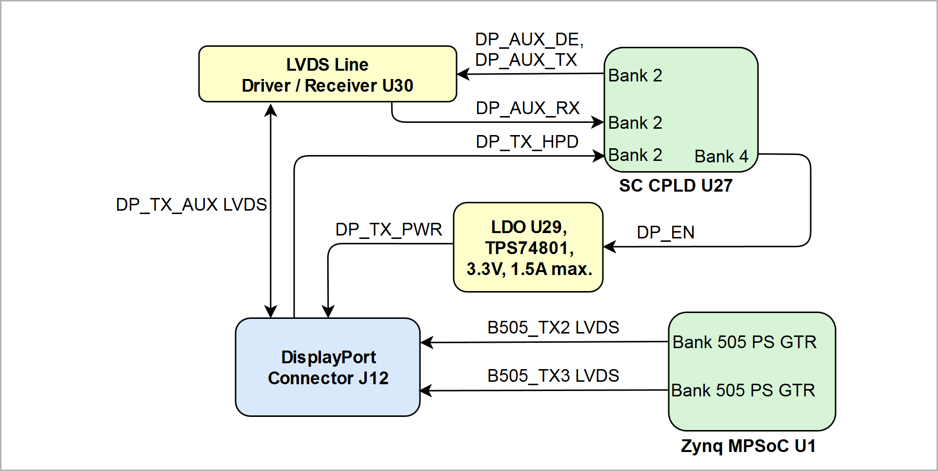 Image Added Image Added
|
|
Follwowing table contains a brief description of the MGT lanes and control and status signals of the DisplayPort interface:
...
| Scroll Title |
|---|
| anchor | Figure_10 |
|---|
| title | Figure 10: DDR4 memory interface |
|---|
|
| Scroll Ignore |
|---|
| draw.io Diagram |
|---|
| border | false |
|---|
| viewerToolbar | true |
|---|
| |
|---|
| fitWindow | false |
|---|
| diagramName | DDR4 memory interface diagram formatted |
|---|
| simpleViewer | false |
|---|
| width | |
|---|
| links | auto |
|---|
| tbstyle | hidden |
|---|
| lbox | true |
|---|
| diagramWidth | 642 |
|---|
| revision | 1 |
|---|
|
|
| Scroll Only |
|---|
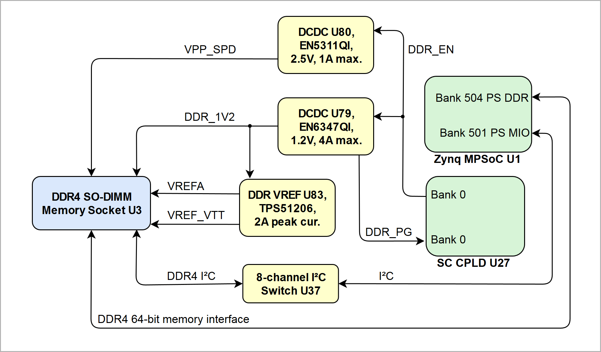 Image Added Image Added
|
|
Following table gives an overview about the I/O signals of the DDR4 SDRAM memory interface:
...
| Scroll Title |
|---|
| anchor | Figure_11 |
|---|
| title | Figure 11: CAN interface |
|---|
|
| Scroll Ignore |
|---|
| draw.io Diagram |
|---|
| border | false |
|---|
| viewerToolbar | true |
|---|
| |
|---|
| fitWindow | false |
|---|
| diagramName | CAN interface diagram formatted |
|---|
| simpleViewer | false |
|---|
| width | |
|---|
| links | auto |
|---|
| tbstyle | hidden |
|---|
| lbox | true |
|---|
| diagramWidth | 641 |
|---|
| revision | 2 |
|---|
|
|
| Scroll Only |
|---|
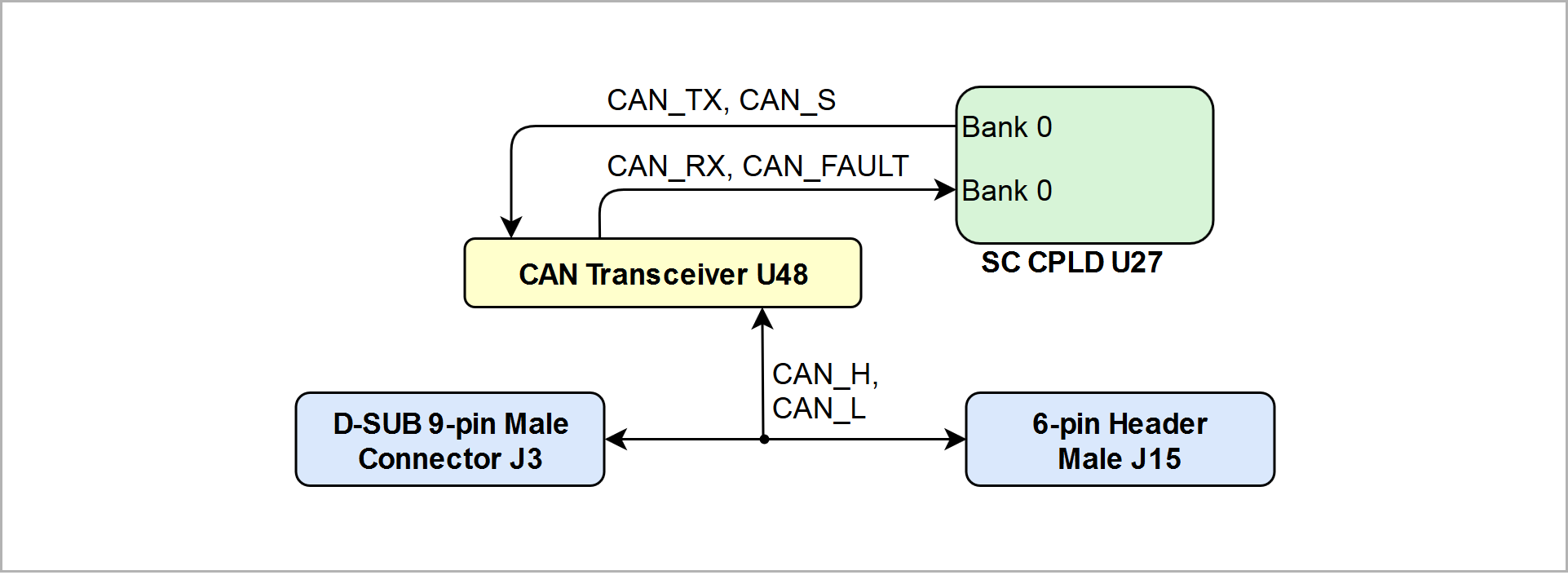 Image Added Image Added
|
|
The CAN interface of external devices can be connected via D-SUB 9-pin male connector J3 or to the 6-pin male header J15:
...
| Scroll Title |
|---|
| anchor | Figure_12 |
|---|
| title | Figure 12: SD Card interface |
|---|
|
| Scroll Ignore |
|---|
| draw.io Diagram |
|---|
| border | false |
|---|
| viewerToolbar | true |
|---|
| |
|---|
| fitWindow | false |
|---|
| diagramName | SD Card interface diagram formatted |
|---|
| simpleViewer | false |
|---|
| width | |
|---|
| links | auto |
|---|
| tbstyle | hidden |
|---|
| lbox | true |
|---|
| diagramWidth | 641 |
|---|
| revision | 1 |
|---|
|
|
| Scroll Only |
|---|
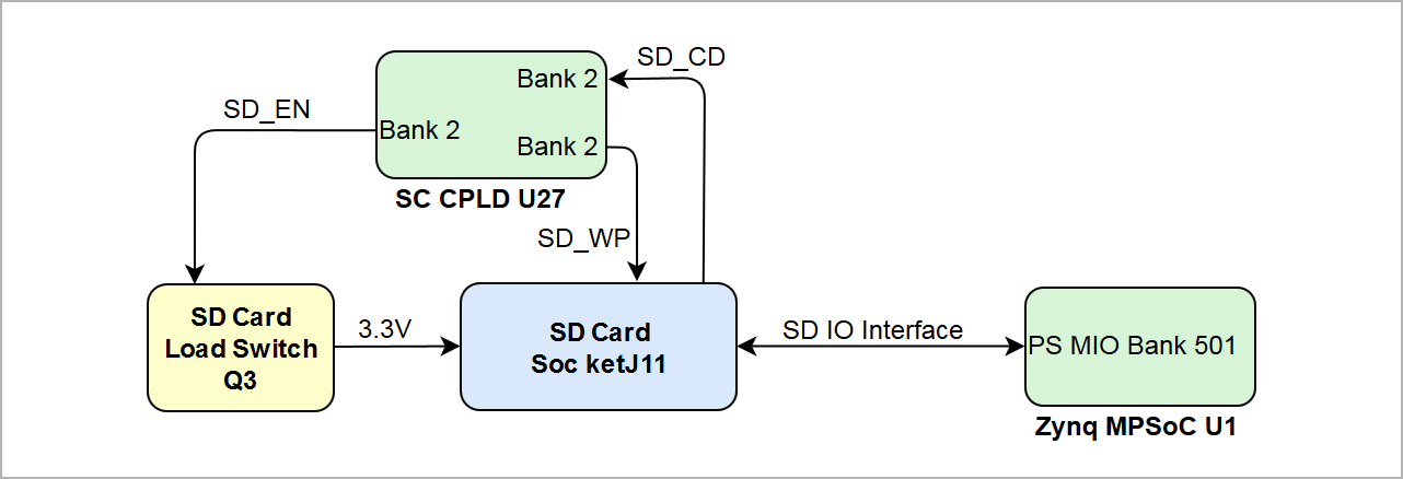 Image Added Image Added
|
|
The SD Card socket have following signal and pin assignment:
...
| Scroll Title |
|---|
| anchor | Figure_13 |
|---|
| title | Figure 13: 4-wire PWM FAN connectors |
|---|
|
| Scroll Ignore |
|---|
| draw.io Diagram |
|---|
| border | false |
|---|
| viewerToolbar | true |
|---|
| |
|---|
| fitWindow | false |
|---|
| diagramName | 4-Wire PWM FAN connectors diagram formatted |
|---|
| simpleViewer | false |
|---|
| width | |
|---|
| links | auto |
|---|
| tbstyle | hidden |
|---|
| lbox | true |
|---|
| diagramWidth | 641 |
|---|
| revision | 3 |
|---|
|
|
| Scroll Only |
|---|
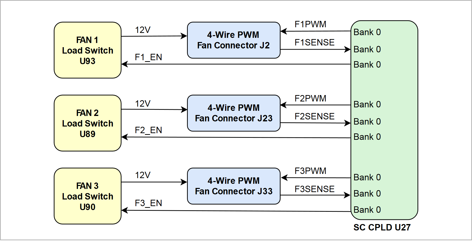 Image Added Image Added
|
|
Following table contains a brief description of the control signals of the fan connectors:
...
| Scroll Title |
|---|
| anchor | Figure_14 |
|---|
| title | Figure 14: PLL clock interface |
|---|
|
| Scroll Ignore |
|---|
| draw.io Diagram |
|---|
| border | false |
|---|
| viewerToolbar | true |
|---|
| |
|---|
| fitWindow | false |
|---|
| diagramName | PLL clock interfaces diagram formatted |
|---|
| simpleViewer | false |
|---|
| width | |
|---|
| links | auto |
|---|
| tbstyle | hidden |
|---|
| lbox | true |
|---|
| diagramWidth | 641 |
|---|
| revision | 3 |
|---|
|
|
| Scroll Only |
|---|
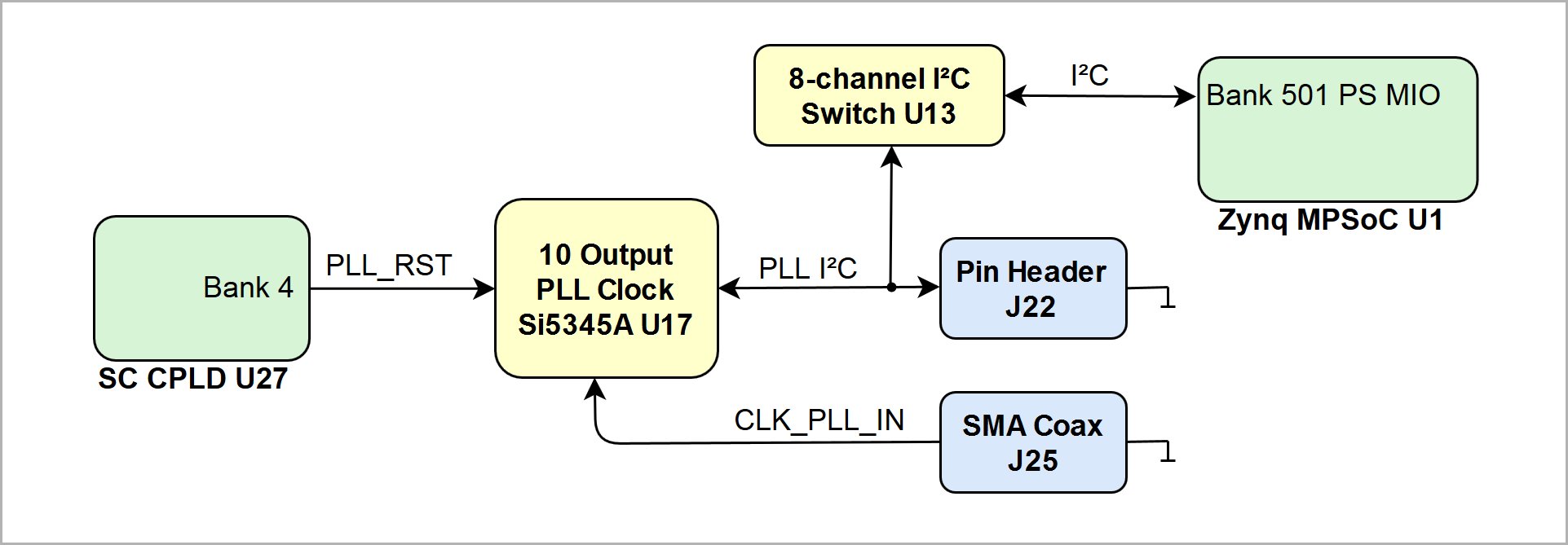 Image Added Image Added
|
|
| Connector | Signal Schematic Name | Connected to | Notes |
|---|
Pin Header J22 | | clock generator U17, pin 16 | PS_1V8 VCCIO
|
| clock generator U17, pin 18 |
SMA Coax J25 | | clock generator U17, pin 1 | - |
...
| Scroll Title |
|---|
| anchor | Figure_15 |
|---|
| title | Figure 15: I/O's connecting Zynq MPSoC and SC CPLD |
|---|
|
| Scroll Ignore |
|---|
| draw.io Diagram |
|---|
| border | false |
|---|
| viewerToolbar | true |
|---|
| |
|---|
| fitWindow | false |
|---|
| diagramName | SC CPLD connections to Zynq MPSoC |
|---|
| simpleViewer | false |
|---|
| width | |
|---|
| links | auto |
|---|
| tbstyle | hidden |
|---|
| lbox | true |
|---|
| diagramWidth | 641 |
|---|
| revision | 1 |
|---|
|
|
| Scroll Only |
|---|
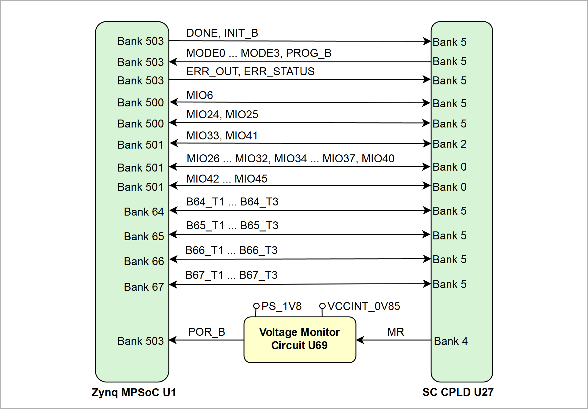 Image Added Image Added
|
|
For detailed information about the current function of the MIO-pin in conjunction with the SC CPLD, the internal signal assignment and implemented logic, refer to the Wiki reference page of the SC CPLD firmware of this board or into the bitstream file of the SC CPLD.
...
| Scroll Title |
|---|
| anchor | Figure_16 |
|---|
| title | Figure 16: Power distribution diagram |
|---|
|
| Scroll Ignore |
|---|
| draw.io Diagram |
|---|
| border | false |
|---|
| viewerToolbar | true |
|---|
| |
|---|
| fitWindow | false |
|---|
| diagramName | Zynq MPSoC CPLD connections |
|---|
| simpleViewer | false |
|---|
| links | auto |
|---|
| tbstyle | hidden |
|---|
| lbox | true |
|---|
| diagramWidth | 641 |
|---|
| revision | 13 |
|---|
|
|
| Scroll Only |
|---|
 Image Added Image Added
|
|
Power distribution to the MPSoC PS and PL units:
| Scroll Title |
|---|
| anchor | Figure_17 |
|---|
| title | Figure 17: Power distribution diagram continued |
|---|
|
| Scroll Ignore |
|---|
| draw.io Diagram |
|---|
| border | false |
|---|
| viewerToolbar | true |
|---|
| |
|---|
| fitWindow | false |
|---|
| diagramName | Power distribution diagram continued |
|---|
| simpleViewer | false |
|---|
| width | |
|---|
| links | auto |
|---|
| tbstyle | hidden |
|---|
| lbox | true |
|---|
| diagramWidth | 641 |
|---|
| revision | 3 |
|---|
|
|
| Scroll Only |
|---|
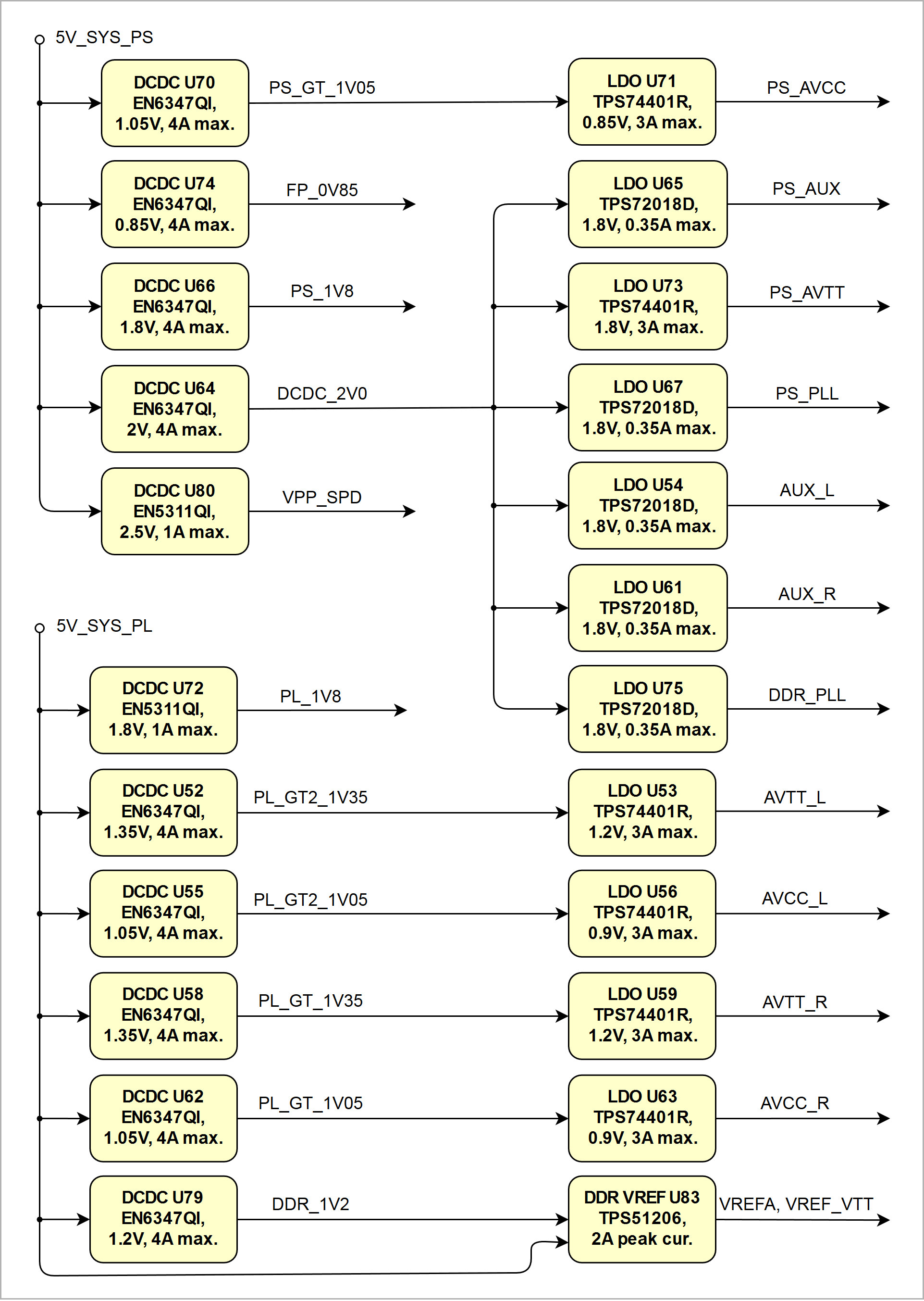 Image Added Image Added
|
|
| Info |
|---|
Note: The DC-DC converter U91 LTM4630EY has an integrated temperature diode for device temperature monitoring. The analog signal 'TEMP_CORE_DC' on pin J6 of the converter is routed to the dedicated differential analog interface (XADC) of the Zynq MPSoC, pin U18 (V_P), pin V17 (V_N) is connected to analog GND. |
...
| Scroll Title |
|---|
| anchor | Figure_18 |
|---|
| title | Figure 18: Power-On sequence diagram |
|---|
|
| Scroll Ignore |
|---|
| draw.io Diagram |
|---|
| border | false |
|---|
| viewerToolbar | true |
|---|
| |
|---|
| fitWindow | false |
|---|
| diagramName | Power-on sequence diagram |
|---|
| simpleViewer | false |
|---|
| width | |
|---|
| links | auto |
|---|
| tbstyle | hidden |
|---|
| lbox | true |
|---|
| diagramWidth | 641 |
|---|
| revision | 2 |
|---|
|
|
| Scroll Only |
|---|
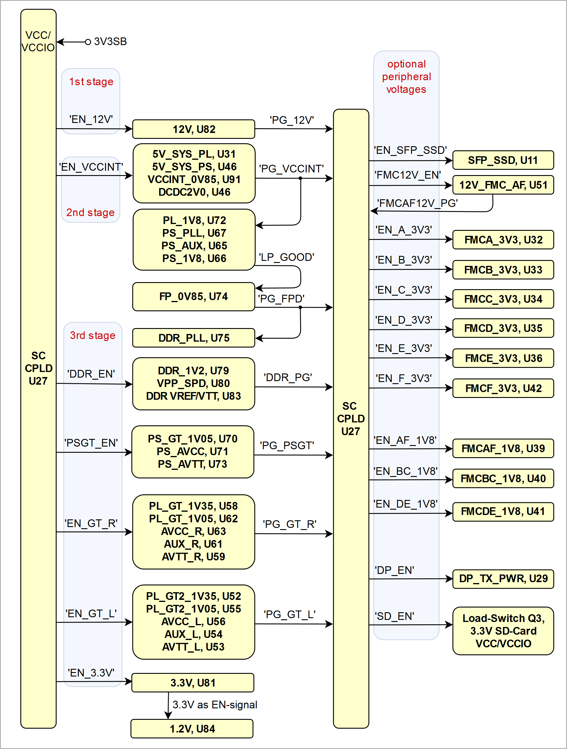 Image Added Image Added
|
|
Power Rails
| Peripheral Designator | VCC / VCCIO Schematic Name | Voltage | Direction | Pins | Notes |
|---|
| J12 | DP_TX_PWR | 3.3V | Out | Pin 20 | Display-Port Connector |
| J9A | SFP_SSD | 3.3V | Out | Pin T15, T16 | SFP+ 2x1 Connector |
| J9B | SFP_SSD | 3.3V | Out | Pin L15, L16 |
| J13A | VBUS1 | 5.0V | Out | Pin U1 | USB3 Ports |
| J13B | VBUS2 | 5.0V | Out | Pin U10 |
| J11 | - | 3.3V | Out | Pin 4 | MicroSD Card Socket |
| B1 | PSBATT | 3.0V | In | Pin + | Battery Holder CR1220 |
| U2 | SSD1_3V3_1 | 3.3V | Out | Pin 2, 4 | SSD PCIe connector |
| SSD1_3V3_2 | 3.3V | Out | Pin 70, 72, 74 |
| SSD1_3V3_3 | 3.3V | Out | Pin 12, 14, 16, 18 |
| U3 | DDR_1V2 | 1.2V | Out | Pin
111, 112, 117, 118, 123, 124,
129, 130, 135, 136, 141, 142,
147, 148, 153, 154, 159, 160,
163 | DDR4 SO-DIMM socket |
| VPP_SPD | 2.5V | Out | Pin 255, 257, 259 |
...