Page History
...
- SFP+ 2x1 cage with integrated LED light pipes, J9
- DisplayPort connector, J12
- USB3 A 2x , RJ45 1x (stacked), J13
- FMC connector (FMC B), J4
- FMC B cooling fan, M2
- FMC connector (FMC C), J8
- FMC C cooling fan, M3
- FMC connector (FMC D), J7
- FMC D cooling fan, M4
- FMC connector (FMC E), J6
- FMC E cooling fan, M5
- I²C programming header of on-board PLL clock generator U17, J22
- 4-Wire PWM fan connector, J23
- Main Power Jack 24V, J1
- CAN bus D-SUB 9-pin male connector, J3
- CAN bus 6-pin header male, J15
- XMOD JTAG header for access to System Controller CPLD, J35
- XMOD JTAG header for access to Zynq MPSoC, J24
- 4-Wire PWM fan connector, J33
- Battery Holder CR1220, B1
- SMA coaxial connector (PLL Si5345A U17 clock input), J25
- Push Button, S1
- Push Button, S2
- DDR4 SO-DIMM socket, U3
- 4-bit DIP-switch, S4
- 4-bit DIP-switch, S3
- FMC connector (FMC A), J10
- FMC A cooling fan, M1
- FMC connector (FMC F), J21
- FMC F cooling fan, M6
- NGFF M.2 PCIe socket (Key M), U2
- SD Card socket, J11
- User LEDs (3x green, 1x red) with LED light pipe, D13 ... D16
- Green LEDs dedicated to USB3 hub U4, D17 ... D19
- Red LED indicating FPGAs 'DONE' signal, D6
- 4-Wire PWM fan connector, J2
- Xilinx Zynq Ultrascale+ MPSoC, U1
...
| Scroll Title | ||||||||||||||||||||||||||||||
|---|---|---|---|---|---|---|---|---|---|---|---|---|---|---|---|---|---|---|---|---|---|---|---|---|---|---|---|---|---|---|
| ||||||||||||||||||||||||||||||
|
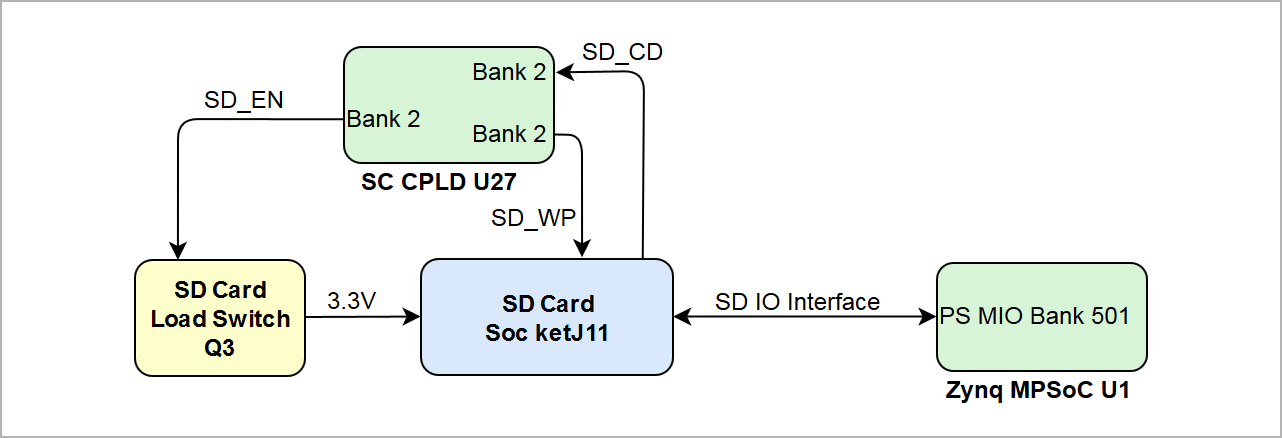
The SD Card socket have following signal and pin assignment:
...
Overview
Content Tools