Page History
...
| PHY Pin | PL bank 34 | B2B | Notes |
|---|---|---|---|
| TX/RX | IO_L1P/IO_L1N | - | |
| CAN_L / CAN_H | - | J1-1 / J1-3 |
Table 8: CAN PHY connections.
I2C Interface
On-board I2C devices are connected to PS MIO28 (SCL) and MIO29 (SDA). I2C addresses for on-board devices are listed in the table below:
| I2C Device | 7bit I2C Address | Notes |
|---|---|---|
| MAC EEPROM, U23 | 0x53 | 1.8V |
| USER EEPROM, U10 | 0x50 | 1.8V |
| Power Management U4 | 0x58 / 0x59 | 3.3V |
| J1 | - | J1-142 SDA, J1-144 SDL at 3.3V |
Table x9: I2C slave device addresses.
...
| HTML |
|---|
<!-- Components on the Module, like Flash, PLL, PHY... --> |
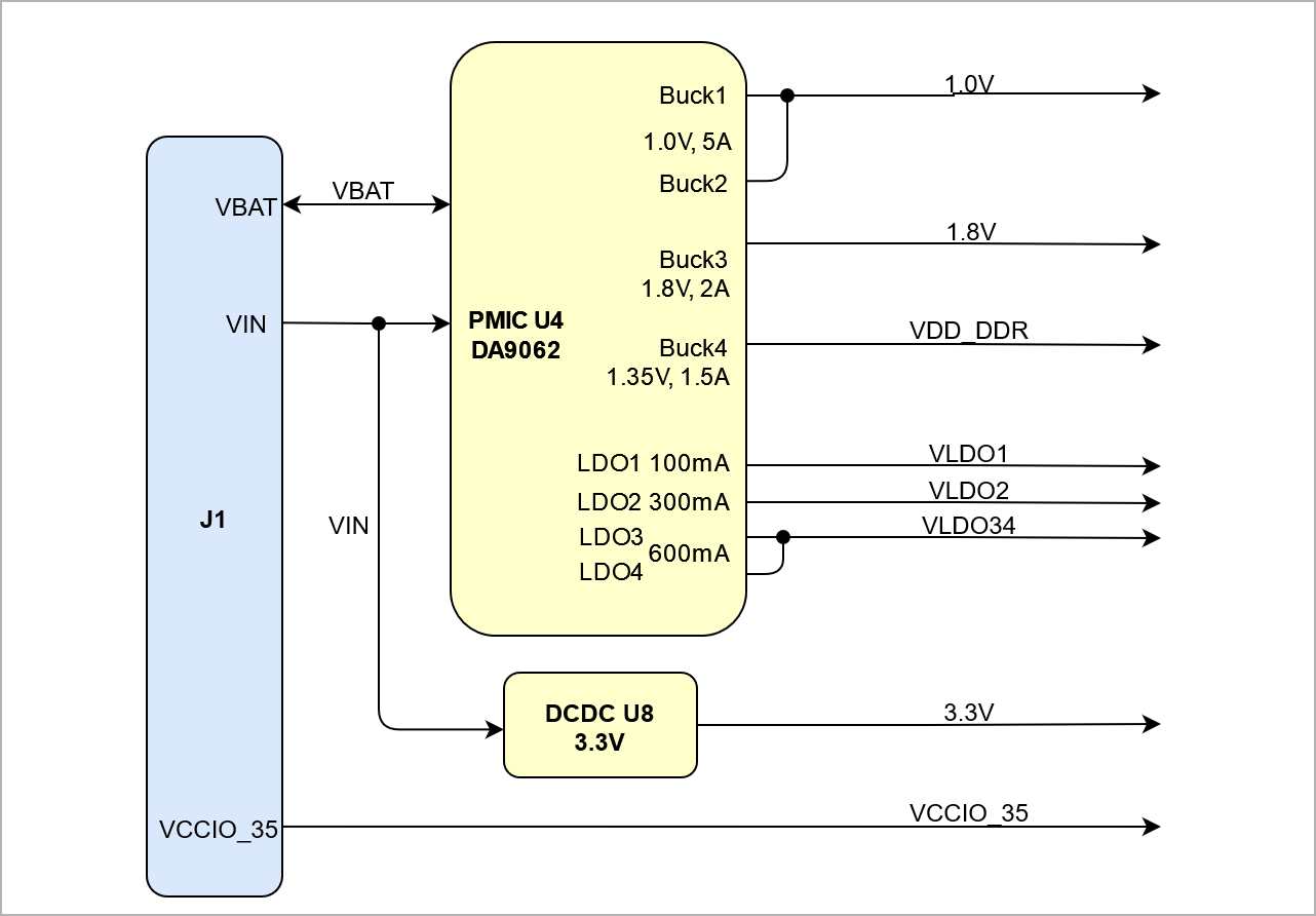
Power Management IC
The Power Management power management IC (U4) is provided by dialog Semiconductors (DA9062). It controls the power-on sequencing of the various power rails. It is preprogrammed and accessible via I2C address 0x58 / 0x59. For a detailed description of the configurable power management IC please refer to the datasheet of dialog semicondutor DA9062.
| HTML |
|---|
<!-- Put in link to the Wiki reference page of the firmware of the SC CPLD. --> |
...
| Clock Source | Schematic Signal | Frequency | Clock Destination |
|---|---|---|---|
| SiTime SiT8008BI oscillator, U9 | ETH_XTAL | 25.000000 MHz | XTAL_IN, U7 ETH PHY |
| SiTime SiT8008AI oscillator, U6 | PS_CLK | 33.333333 MHz | PS_CLK_500, Bank 500 |
Table Table10 : Reference clock signals.
...
| LED | Color | Connected to | Description and Notes |
|---|---|---|---|
| D1 | Green | PS MIO7 | User LED. |
| D2 | Green | PL IO_L3P_T0_34 | User LED. |
| D3 | Red | PL IO_L4N_T0_34 | User LED. |
Table 11: On-board LEDs.
Power and Power-On Sequence
...
| Power Input | Typical Current |
|---|---|
| VIN | TBD* |
| 3.3VIN | TBD* |
Table 12: Typical power consumption.
...
Power supply with minimum current capability of ...A for system startup is recommended.
For the lowest power consumption and highest efficiency of the The on-board DC-DC regulators it is recommended to power the module from one single 3.3V supply. All input power supplies have a nominal value of 3.3V. Although the input power supplies can be powered up in any order, it is recommended to power them up simultaneously.The on-board voltages of the TE0724 SoC module will be voltages of the TE0724 SoC module will be powered-up in order of a determined sequence after the external voltages '...', '...' and '...' are availableVIN is available and nONKEY is asserted.
| Warning |
|---|
| To avoid any damage to the module, check for stabilized on-board voltages should be carried out (i.e. power good and enable signals) before powering up any SoC's I/O bank voltages VCCO_x. All I/Os should be tri-stated during power-on sequence. |
Power Distribution Dependencies
| Scroll Title | ||||
|---|---|---|---|---|
|
...
| ||||||||||||||||||||||
|
See Xilinx data sheet ... for additional information. User should also check related base board documentation when intending base board design for TE07xx TE0724 module.
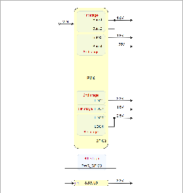
Power-On Sequence
The TE07xx TE07024 SoM meets the recommended criteria to power up the Xilinx Zynq MPSoC properly by keeping a specific sequence of enabling the on-board DC-DC converters dedicated to the particular functional units of the Zynq chip and powering up the on-board voltages. For a detailed description of the configurabel Power Management IC please refer to the datasheet of dialog semicondutor DA9062.
Following diagram clarifies the sequence of enabling the particular on-board voltages, which will power-up in descending order as listed in the blocks of the diagram:
Put power-on diagram here...
...
| Scroll Title | ||||
|---|---|---|---|---|
|
...
Voltage Monitor Circuit
If the module has one, describe it here...
Power Rails
...
|
Power Rails
Power Rail Name | B2B JM1 Pins | B2B JM2 Pins | Direction | Notes | |
|---|---|---|---|---|---|
| VIN | 1, 3, 5 | 2, 4, 6, 8 | Input | Main supply voltage from the carrier board. | |
| 3.3V | - | 10, 12, 91 | Output | Module on-board 3.3V voltage supply. (would be good to add max. current allowed here if possible) | |
| B64_VCO | 9, 11 | - | InputHR (High Range) bank voltage supply from the carrier board. | ||
VBAT_IN | 79 | - | Input | RTC battery supply voltage from the carrier board. | |
| ... | ... | ... | ... | ... |
Table 13: Module power rails.Different modules (not just 4 x 5 cm ones) have different type of connectors with different specifications. Following note is for Samtec Razor Beam™ LSHM connectors only, but we should consider adding such note into included file in Board to Board Connectors section instead of here.
...
Current rating of
...
Samtec connectors is
...
1.
...
5A per pin (2 adjacent pins powered).
Bank Voltages
Bank | Schematic Name | Voltage | Voltage Range |
|---|---|---|---|
| 500 (MIO0) | PS_1.8V | 1.8V | - |
| 501 (MIO1) | PS_1.8V | 1.8V | - |
| 502 (DDR3) | 1.35V | 1.35V | - |
| 12 HR | VCCIO_12 | User | HR: 1.2V to 3.3V |
| 13 HR | VCCIO_13 | User | HR: 1.2V to 3.3V |
| 33 HP | VCCIO_33 | User | HP: 1.2V to 1.8V |
| 34 HP | VCCIO_34 | User | HP: 1.2V to 1.8V |
| 35 HP | VCCIO_35 | User | HP: 1.2V to 1.8V |
Table 14: Module PL I/O bank voltages.
...
| HTML |
|---|
<!-- Set correct link to the overview table of the product on english and german, if not available, set https://shop.trenz-electronic.de/de/Produkte/Trenz-Electronic/ https://shop.trenz-electronic.de/en/Products/Trenz-Electronic/ --> |
| Trenz shop TE0xxx TE0724 overview page | |
|---|---|
| English page | German page |
...
Overview
Content Tools