Page History
...
| Scroll Title | ||||||||||||||||||||||||||||||||||||||||||||||||||||||
|---|---|---|---|---|---|---|---|---|---|---|---|---|---|---|---|---|---|---|---|---|---|---|---|---|---|---|---|---|---|---|---|---|---|---|---|---|---|---|---|---|---|---|---|---|---|---|---|---|---|---|---|---|---|---|
| ||||||||||||||||||||||||||||||||||||||||||||||||||||||
|

...
| Scroll Title | ||||||||||||||||||||||||||||||
|---|---|---|---|---|---|---|---|---|---|---|---|---|---|---|---|---|---|---|---|---|---|---|---|---|---|---|---|---|---|---|
| ||||||||||||||||||||||||||||||
|
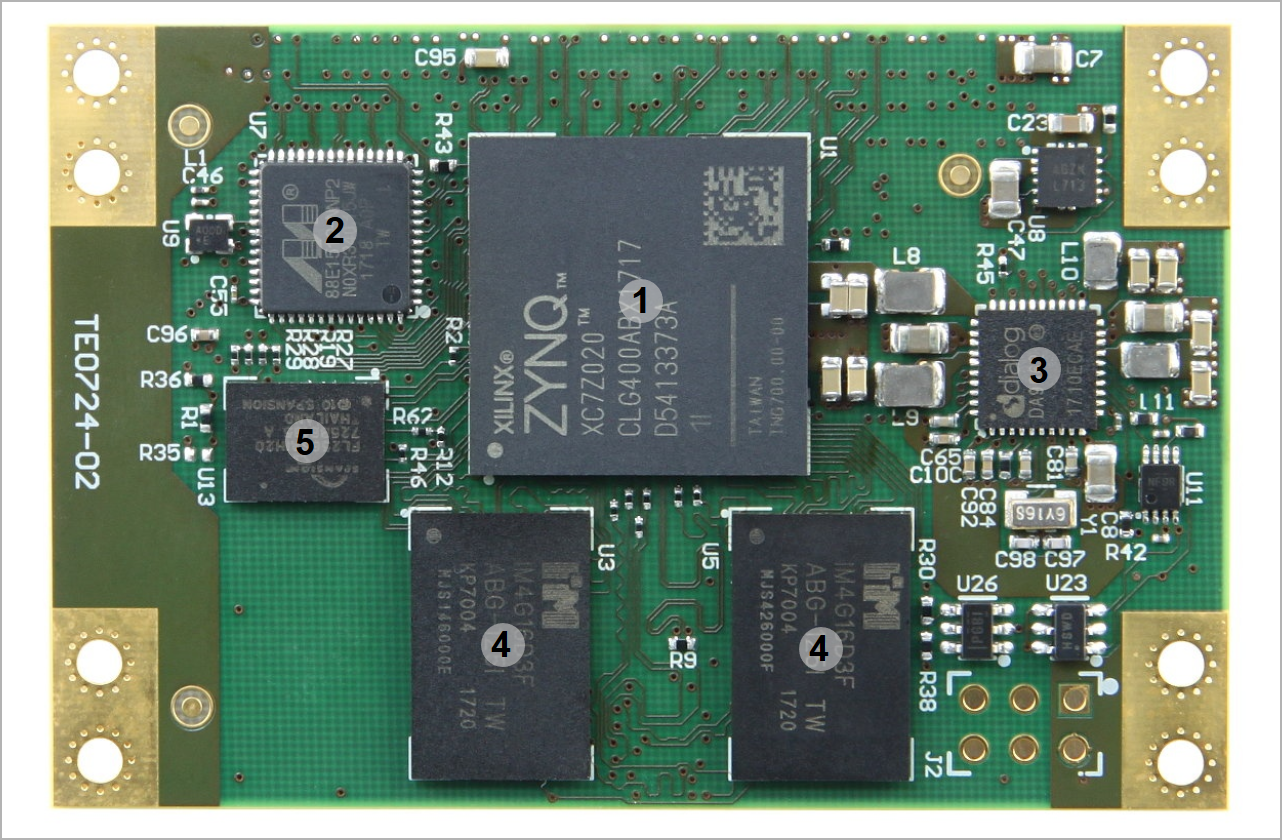
See Xilinx data sheet for additional information. User should also check related base board documentation when intending base board design for TE0724 module.
...
| Scroll Title | |||||||||||||||||||||||||||||||
|---|---|---|---|---|---|---|---|---|---|---|---|---|---|---|---|---|---|---|---|---|---|---|---|---|---|---|---|---|---|---|---|
| |||||||||||||||||||||||||||||||
|
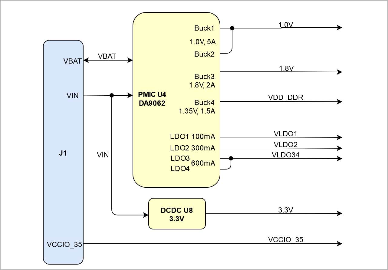
Power Rails
Power Rail Name | B2B JM1 PinsB2B JM2 Pins | Direction | Notes | ||
|---|---|---|---|---|---|
| VIN1 | 154, | 3156, | 52, 4, 6, 8158,160 | Input | Main supply voltage from the carrier board. |
| 3.3V | - | 10, 12, 91 | Output | Module on-board 3.3V voltage supply. (would be good to add max. current allowed here if possible) | 9, 11 | - | Input |
| VCCIO_35 | 54 | Input | PL Bank 35 supply voltage. | ||
| VLDO1 | 83 | Output | |||
| VLDO2 | 94 | Output | |||
| VLDO34 | 53 | Output | |||
| 3.3V | 43, 74 | Output | Module on-board 3.3V voltage supply. | ||
| 1.0V | - | Buck1 & Buck2 of U4. | |||
| 1.8V | - | Buck3 of U4. | |||
| VDD_DDR | - | DDR supply voltage powered by Buck4 of U4. | |||
VBAT | 152 | Output | Battery charger to the carrier board. | ||
VBAT_IN | 79 | - | Input | RTC battery supply voltage from the carrier board. | |
| ... | ... | ... | ... | ... |
Table 13: Module power rails.
Current rating of Samtec connectors theSamtec connector is 1.5A per pin (2 adjacent pins powered1 pin powered per row).
Bank Voltages
Bank | Schematic Name | Voltage | Voltage Range |
|---|---|---|---|
| 500 (MIO0)MIO | PS_1.8V | 1.8V | - |
| 501 (MIO1) | PS_1.8V | 1.8V | - |
| 502 (DDR3) | 1.35V | 1.35V | - |
| 12 HR | VCCIO_12 | User | HR: 1.2V to 3.3V |
| 13 HR | VCCIO_13 | User | HR: 1.2V to 3.3V |
| 33 HP | VCCIO_33 | User | HP: 1.2V to 1.8V |
| 34 HP | VCCIO_34 | User | HP: 1.2V to 1.8V |
| 501 MIO | 1.8V | 1.8V | - |
| 502 DDR3 | VDD_DDRV | 1.35V | - |
| 34 HP | 3.3V | 3.3V | - |
| 35 HP | VCCIO_35 | User | HP: 1.2V to 13.83V |
Table 14: Module PL I/O bank voltages.
...
Parameter | Min | Max | Units | Reference Document |
|---|---|---|---|---|
VIN supply voltage | V | - | ||
Storage temperature | -40 | 85 | °C | - |
Table 15: Module absolute maximum ratings.
...
| Parameter | Min | Max | Units | Reference Document |
|---|---|---|---|---|
| VIN supply voltage | V | |||
| Operating temperature | -40 | 85 | °C |
Table 16: Module recommended operating conditions.
...
| Date | Revision | Notes | PCN | Documentation Link |
|---|---|---|---|---|
| - | 01 | Prototypes | ||
| 02 |
Table : Module hardware revision history.
...
Overview
Content Tools