Page History
...
| Scroll Title | ||||||||||||||||||||||||||||||
|---|---|---|---|---|---|---|---|---|---|---|---|---|---|---|---|---|---|---|---|---|---|---|---|---|---|---|---|---|---|---|
| ||||||||||||||||||||||||||||||
|
| HTML |
|---|
<!-- MGT lanes should be listed separately, as they are more specific than just general I/Os. --> |
...
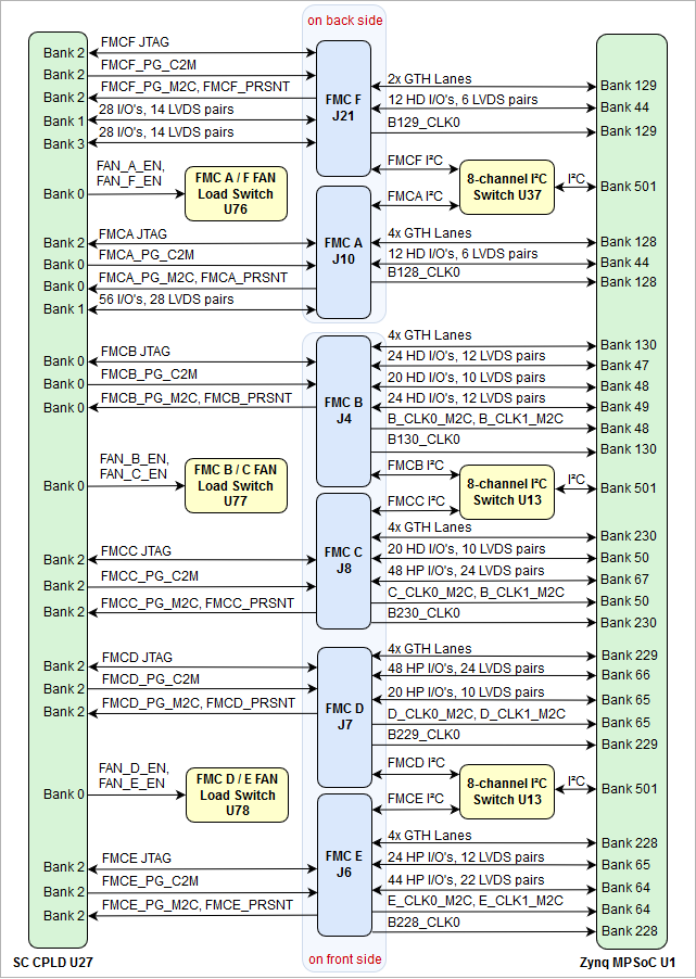
| FMC | Interfaces | I/O Signal Count | LVDS-pairs count | Connected to | VCCO bank Voltage | Notes |
|---|---|---|---|---|---|---|
J21 (FMC F) | I/O | 12 | 6 | Bank 44 HD | FMCAF_1V8 | - |
| 28 | 14 | SC CPLD U27 Bank 1 | FMCAF_1V8 | - | ||
| 6828 | 3414 | SC CPLD U27 Bank 3 | FMCAF_1V8 | - | ||
| I²C | 2 | - | I²C-Switch U37 | - | Muxed to MIO Bank 501 I²C Inteface | |
| JTAG | 4 | - | SC CPLD U27 Bank 2 | 3.3VSB | - | |
| MGT | - | 4 (2 x RX/TX) | Bank 129 GTH | - | 2x MGT lanes | |
| Clock Input | - | 1 | Bank 129 GTH | - | 1x Reference clock input to MGT bank | |
| Control Signals | 3 | - | SC CPLD U27 Bank 2 | 3.3VSB | 'FMCF_PG_C2M', 'FMCF_PG_M2C', 'FMCF_PRSNT' |
...
Overview
Content Tools