Page History
...
| Scroll Title | ||||||||||||||||||||||||||||||||||||||||||||||||||||||||||||
|---|---|---|---|---|---|---|---|---|---|---|---|---|---|---|---|---|---|---|---|---|---|---|---|---|---|---|---|---|---|---|---|---|---|---|---|---|---|---|---|---|---|---|---|---|---|---|---|---|---|---|---|---|---|---|---|---|---|---|---|---|
| ||||||||||||||||||||||||||||||||||||||||||||||||||||||||||||
|
...
- Module connector for 4,0x6.0 cm module
- Pmods usabel as dual Pmods, J10, J11, J12, J13, J14, J15, J16, J17
- Pmod (single), J20
- I2C Pmod, J21
- CAN screw terminal, J2
- 5V 2.1mm input jack, J18
- microUSB J4
- USB to JTAG/UART bridge FT2232H, U1
- Configuration EEPROM U3
- RJ45 Gigabit Ehternet Jack, J3
- Power Button, S1
- Reset Button, S3
- User Button PS, S5
- User LED (green) PS, D8
- 2x User Button PL, S2, S4
- 6x User LEDs (red) PL, D2-D7
- Power LED (green), D36
- 2x10 Pin header for Boot and Programming options, J6
- 2x6 Pin header for CAN bus termination resistors jumper setting vb
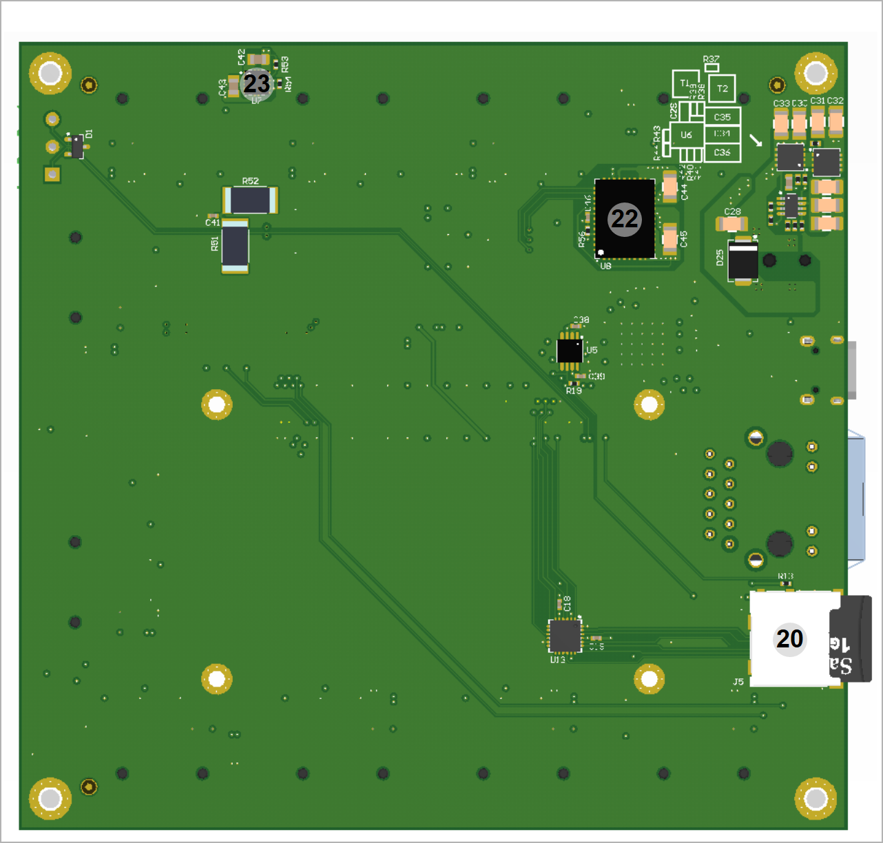
- microSD Card Slot, J5
Initial Delivery State
...
The GPIOs of the 10 Pmods (J10 to J17, J20, J21) are connected with 100 Ohm differential routing to the B2B connector.J21 is a pure I2C compatible Pmod, without additional signals. The other 9 are GPIO Pmods where despite J20 all others can be used as dual Pmods. By default VCCIO_35 is connected with a 0 Ohm resistor to 3.3V. De-soldering this resistor and using pinheader J19 instead, the variable bank power VCCIO_35 for the Pmods J10, J11, J12, J13, J14, J16 can be selected.
| J10 | J11 | J12 | J13 | J14 | J15 | J16 | J17 | J20 | J21 | |||||||||||
|---|---|---|---|---|---|---|---|---|---|---|---|---|---|---|---|---|---|---|---|---|
| PIN | Signal | B2B | Signal | B2B | Signal | B2B | Signal | B2B | Signal | B2B | Signal | B2B | Signal | B2B | Signal | B2B | Signal | B2B | Signal | B2B |
| 1 | PA0_P | J1-56 | PB2_N | J1-70 | PC2_P | J1-57 | PD2_P | J1-77 | PE2_N | J1-90 | PG2_N | J1-110 | PF2_P | J1-97 | PH2_P | J1-115 | PI2_P | J1-133 | NC | - |
| 2 | PA0_N | J1-58 | PB2_P | J1-72 | PC2_N | J1-55 | PD2_N | J1-75 | PE2_P | J1-92 | PG2_P | J1-112 | PF2_N | J1-95 | PH2_N | J1-113 | PI2_N | J1-131 | NC | - |
| 3 | PA3_P | J1-46 | PB0_N | J1-76 | PC0_P | J1-51 | PD0_P | J1-71 | PE0_N | J1-96 | PG0_P | J1-114 | PF0_P | J1-91 | PH0_P | J1-111 | PI0_P | J1-129 | I2C_SCL | J1-142 |
| 4 | PA3_N | J1-48 | PB0_P | J1-78 | PC0_N | J1-49 | PD0_N | J1-69 | PE0_P | J1-98 | PG0_N | J1-116 | PF0_N | J1-89 | PH0_N | J1-109 | PI0_N | J1-127 | I2C_SDA | J1-144 |
| 5 | GND | - | GND | - | GND | - | GND | - | GND | - | GND | - | GND | - | GND | - | GND | - | GND | - |
| 6 | VCCIO_35 | J1-54 | VCCIO_35 | J1-54 | VCCIO_35 | J1-54 | VCCIO_35 | J1-54 | VCCIO_35 | J1-54 | 3.3V | J1-74, J1- 43 | VCCIO_35 | J1-54 | 3.3V | J1-74, J1- 43 | 3.3V | J1-74, J1- 43 | 3.3V | J1-74, J1- 43 |
| 7 | PA1_N | J1-62 | PB3_P | J1-68 | PC3_N | J1-59 | PD3_N | J1-79 | PE3_P | J1-88 | PG3_P | J1-108 | PF3_N | J1-99 | PH3_N | J1-117 | PI3_N | J1-135 | NC | - |
| 8 | PA1_P | J1-60 | PB3_N | J1-66 | PC3_P | J1-61 | PD3_P | J1-81 | PE3_N | J1-86 | PG3_N | J1-106 | PF3_P | J1-101 | PH3_P | J1-119 | PI3_P | J1-137 | NC | - |
| 9 | PA2_N | J1-52 | PB1_P | J1-82 | PC1_N | J1-45 | PD1_N | J1-65 | PE1_P | J1-102 | PG1_N | J1-120 | PF1_N | J1-85 | PH1_N | J1-105 | PI1_N | J1-123 | I2C_SCL | J1-142 |
| 10 | PA2_P | J1-50 | PB1_N | J1-80 | PC1_P | J1-47 | PD1_P | J1-67 | PE1_N | J1-100 | PG1_P | J1-121 | PF1_P | J1-87 | PH1_P | J1-107 | PI1_P | J1-125 | I2C_SDA | J1-144 |
| 11 | GND | - | GND | - | GND | - | GND | - | GND | - | GND | - | GND | - | GND | - | GND | - | GND | - |
| 12 | VCCIO_35 | J1-54 | VCCIO_35 | J1-54 | VCCIO_35 | J1-54 | VCCIO_35 | J1-54 | VCCIO_35 | J1-54 | 3.3V | J1-74, J1- 43 | VCCIO_35 | J1-54 | 3.3V | J1-74, J1- 43 | 3.3V | J1-74, J1- 43 | 3.3V | J1-74, J1- 43 |
Table 9: Pmod connections.
...
| PIN | Signal | B2B |
|---|---|---|
| J2-1 | CAN0_N | J1-1 |
| J2-2 | GND | |
| J2-3 | CAN0_P | J1-3 |
Table 910: CAN bus connection.
Proper termination of the can bus can be set via jumpers on J22 according to the device position on the bus. Jumpers on J22-1 to J22-3 and J22-2 to J22-4 connect proper split termination resistors to the CAN bus.
...
| Clock Source | Schematic Name | Frequency | Clock Destination |
|---|---|---|---|
| SiTime SiT8008AI oscillator, U4 | OSCI | 12.000000 MHz | U1, pin 3. |
Table 911: Reference clock signals.
...
| LED | Color | Signal | Description and Notes |
|---|---|---|---|
| D1 | green | VIN | power indicator |
| D2-D7 | red | ULED1..6 | User LED |
| D8 | green | MIO9 | MIO user LED |
| J3B | green | PHY_LED0 | Ethernet status |
| J3C | yellow | PHY_LED1 | Ethernet status |
Table 1012: On-board LEDs.
On-board Push Buttons
| Button | Signal | B2B | Description and Notes |
|---|---|---|---|
| S1 | ONKEY | J1-148 | Power Button, pulled up, on push de-asserted |
| S3 | RESETREQ | J1-150 | User LED pulled up, on push de-asserted |
S2 | S2 | J1-124 | PL user button, pulled up, on push de-asserted |
| S4 | S4 | J1-126 | PL user button, pulled up, on push de-asserted |
| S5 | MIO51 | J1-42 | PS MIO user button, pulled up, on push de-asserted |
Table 1113: On-board Push Buttons.
Pin Header
...
| PIN | Signal | B2B |
|---|---|---|
| J6-1 | VIN | J1-154, J1-156, J1-158, J1-160 |
| J6-2 | VIN | J1-154, J1-156, J1-158, J1-160 |
| J6-3 | GND | |
| J6-4 | GND | |
| J6-5 | I2C_SCL | J1-142 |
| J6-6 | VBAT | J1-152 |
| J6-7 | I2C_SDA | J1-144 |
| J6-8 | PWR_GPIO2 | J1-143 |
| J6-9 | ONKEY | J1-148 |
| J6-10 | PWR_GPIO4 | J1-141 |
| J6-11 | PWR_TP | J1-146 |
| J6-12 | RESETREQ | J1-150 |
| J6-13 | MODE0 | J1-2 |
| J6-14 | GND | |
| J6-15 | MODE1 | J1-4 |
| J6-16 | GND |
Table 1214: Pin Header J6.
For voltage selection VCCIO_35 of (SoM TE0724, Bank 35) other than 3.3V the header J19 can optionaly assembled. Therefore 0 Ohm resistor R45 has to be removed!
| PIN | Signal | B2B |
|---|---|---|
| J19-1 | VLDO1 | J1-83 |
| J19-2 | GND | |
| J19-3 | VCCIO_35 | J1-54 |
| J19-4 | VLDO2 | J1-94 |
J19-5 | VLDO34 | J1-53 |
| J19-6 | GND |
Table 1315: Optional Pin Header J19.
...
| PIN | Signal | B2B |
|---|---|---|
| J8-1 | 3.3V | J1-43, J1-74 |
| J8-2 | GND | |
| J8-3 | S4 | J1-126 |
| J8-4 | S2 | J1-124 |
| J8-5 | ULED5 | J1-130 |
| J8-6 | ULED6 | J1-128 |
| J8-7 | ULED3 | J1-134 |
| J8-8 | ULED4 | J1-132 |
| J8-9 | ULED1 | J1-138 |
| J8-10 | ULED2 | J1-136 |
Table 1416: Optional Pin Header J8.
Optional pin header J7 gives access to otherwise not used PS MIO IOs at a 3.3V bank.
| PIN | Signal | B2B |
|---|---|---|
| J7-1 | 3.3V | 43, 74 |
| J7-2 | GND | |
| J7-3 | GND | |
| J7-4 | MIO8 | J1-14 |
| J7-5 | MIO10 | J1-31 |
| J7-6 | MIO11 | J1-33 |
| J7-7 | MIO12 | J1-35 |
| J7-8 | MIO13 | J1-37 |
| J7-9 | MIO14 | J1-39 |
| J7-10 | MIO15 | J1-41 |
Table 1517: Optional Pin Header J7.
Optional pin header J9 gives access to otherwise not used PS MIO IOs at a 1.8V bank.
| PIN | Signal | B2B |
|---|---|---|
| J9-1 | 1.8V | J1-63 |
| J9-2 | GND | |
| J9-3 | GND | |
| J9-4 | MIO_46 | J1-32 |
| J9-5 | MIO_50 | J1-40 |
| J9-6 | MIO_PB | J1-42 |
Table 1618: Optional Pin Header J9.
Power and Power-On Sequence
...
| Power Input | Typical Current |
|---|---|
| VIN | TBD* |
Table 1719: Typical power consumption.
...
The power-on sequence is solely controlled by the attached module. Optional sequenzing signals for integration of additional hardware are PWR_GPIO2 and PWR_GPIO4. If the attached module uses the adjustable bank power VCCIO_35, this has to be powered up after the modules SOCs powerrails are up and before any other signal is applied to the bank IOs.
The 1.8V and 3.3V power rails are used for the SD Card level shifter U13. The Datasheet states to first power up 1.8V and then 3.3V.
Power Rails
, this has to be taken into account when reconfiguring the power circuit of the SoM.
Power Rails
Power Rail Power Rail Name | B2B J1 Pins | Direction on B2B | Notes |
|---|---|---|---|
| VIN | 154, 156, 158, 160 | Output | External main supply voltage. |
| 3.3V | 43, 74 | Input | |
1.8V | 63 | Input | |
| VCCIO_35 | 54 | Output | |
VLDO1 | 83 | Input | |
| VLDO2 | 94 | Input | Used to enable UART level shifter. Therefore fix at 1.8V. |
| VLDO34 | 53 | Input | |
VBAT | 152 | Input/Output | Reserved for PMIC backup battery and charger. |
Table 18 20 : Board power rails.
Board to Board Connectors
...
Order | REF Number | Samtec Number | Type | Mated Height | Data sheet | Comment |
|---|---|---|---|---|---|---|
| - | REF-192552-01 | SS5-80-3.50-L-D-K-TR | Baseboard connector | 4 mm | http://suddendocs.samtec.com/catalog_english/ss5.pdf | Standard connector used on board |
| 27220 | REF-192552-02 | ST5-80-1.50-L-D-P-TR | Module connector | 4 mm | http://suddendocs.samtec.com/catalog_english/st5.pdf | Standard connector used on module |
Table 1921: Connectors for module and base board.
...
Parameter | Min | Max | Units | Reference Document | |
|---|---|---|---|---|---|
VIN supply voltage | -0.3 | V | 5.5 | V | Depends mostly on attached SoM, values here are for TE0724 PMIC, da9062_3v4.pdf.- |
Storage temperature | -30 | 80 | °C - | Push buttons datasheet. |
Table 20: Board absolute maximum ratings.
...
Recommended Operating Conditions
| Parameter | Min | Max | Units | Reference Document |
|---|---|---|---|---|
| VIN supply voltage | 0 | 5.5 | V | Depends mostly on attached SoM, values here are for TE0724 PMIC, da9062_3v4.pdf. |
| Operating temperature | -25 | 70 | °C | Push buttons datasheet. |
Table 21: Board recommended operating conditions.
| Note |
|---|
| Please check Xilinx datasheet ... also the attached SOMs datasheet for complete list of absolute maximum and recommended operating ratings. |
...
| Scroll Title | ||
|---|---|---|
| ||
Revision History
...
Overview
Content Tools