Page History
...
| Scroll Title | ||||||||||||||||||||||||||||||
|---|---|---|---|---|---|---|---|---|---|---|---|---|---|---|---|---|---|---|---|---|---|---|---|---|---|---|---|---|---|---|
| ||||||||||||||||||||||||||||||
|
| HTML |
|---|
<!-- MGT lanes should be listed separately, as they are more specific than just general I/Os. --> |
...
| Connector | Interface | Signal Schematic Name | Connected to | Notes |
|---|---|---|---|---|
M.2-NGFF PCIe Socket U2 | MGT Lane |
| PS_MGTRTXP0_505, AB29 | Multi gigabit highspeed TX: Output RX: Input |
| Clock Input |
| Quad programmable PLL clock generator U12, CLK0 | Reference clock signal | |
| Control Lines |
| SC CPLD U27, bank 2, pin AA13 | LED, Output, High active | |
| SC CPLD U27, bank 2, pin AA12 | PCIe sleep state, Input, Low active | ||
| SC CPLD U27, bank 2, pin AA11 | PCIe reset input, Input, Low active | ||
| SC CPLD U27, bank 2, pin AB11 | PCIe Link reactivation, Input, Low active | ||
| connect to GND | PCIe Clock Request, Low active |
...
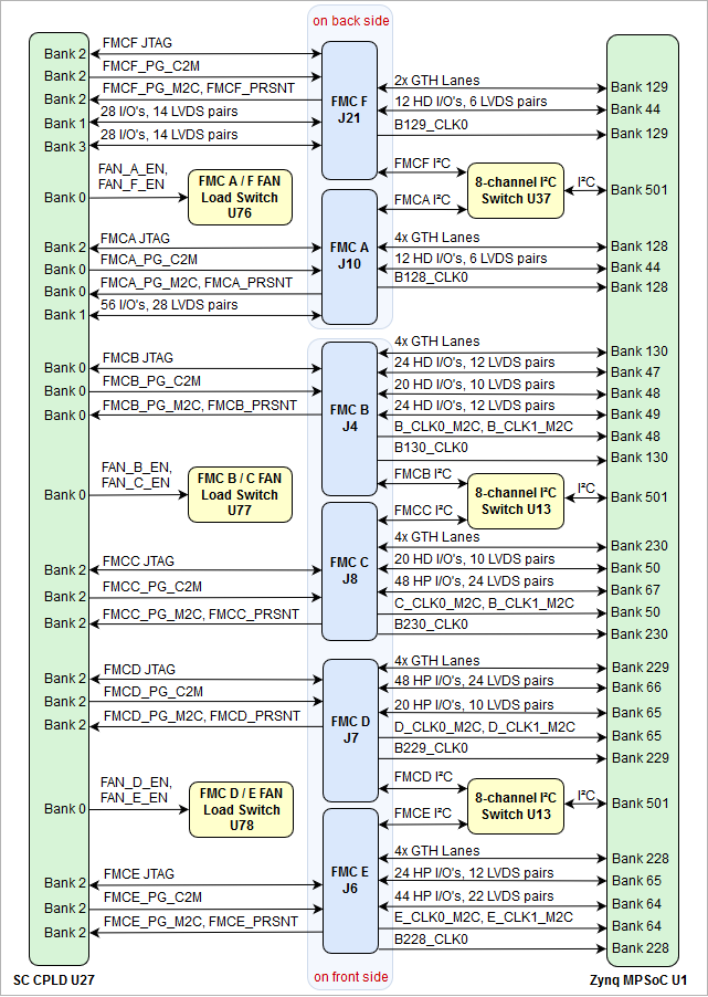
The TEB0911 carrier board contains several EEPROMs for configuration and general user purposes. The EEPROMs are provided by Microchip and all have , the I²C interfaces of the EEPROM's are multiplexed to the I²C switch U37:
| EEPROM Modell | Designator | Memory Density | Purpose |
|---|---|---|---|
| 24LC128-I/ST | U57 | 128 Kbit | user |
| 24AA025E48T-I/OT | U60 | 2 Kbit | user |
| 24AA025E48T-I/OT | U45 | 2 Kbit | user |
| 24AA025E48T-I/OT | U83 | 2 Kbit | user |
| 24LC128-I/ST | U5 | 128 Kbit | USB3 Hub U4 configuration memory |
...
| Clock Source | Signal Schematic Name | Frequency | Clock Input Destination |
|---|---|---|---|
| SiTime SiT8008BI oscillator, U22 |
| 33.333333 MHz | Zynq MPSoC PS Config Bank 503, pin U24 |
| SiTime SiT8008AI oscillator, U16 |
| 52.000000 MHz | USB2 transceiver PHY U15, pin 26 |
| Kyocera CX3225SB26000, Y3 | - | 26.000 MHz | 4-port USB3 Hub U4, pin 68/69 |
| Kyocera CX3225SB26000, Y2 |
| 54.000 MHz | PLL clock generator U17, pin 8/9 |
| SiTime SiT8008BI oscillator, U21 |
| 25.000000 MHz | Gigabit Ethernet PHY U20, pin 34 |
SiTime SiT8008AI oscillator, U87 optional, not equipped |
| 25.000000 MHz | System Controller CPLD U27, bank 2, pin AA9 |
| SiTime SiT8008BI oscillator, U18 |
| 25.000000 MHz | PLL clock generator U17, pin 63 |
| SiTime SiT8008AI oscillator, U85 | - | 25.000000 MHz | PLL clock generator U12, pin 3 |
DSC1123 oscillator, U92 optional, not equipped |
| 100.0000 MHz | PS GTR Bank 505 Lane 3, dedicated for DisplayPort, Pin pin U31, U32 |
Table 50: Reference clock signal oscillators
...
Overview
Content Tools