Page History
...
| Scroll Title | ||||||||||||||||||||||||||||||||||
|---|---|---|---|---|---|---|---|---|---|---|---|---|---|---|---|---|---|---|---|---|---|---|---|---|---|---|---|---|---|---|---|---|---|---|
| ||||||||||||||||||||||||||||||||||
|
Main Components
| Scroll Title | ||||||||||||||||||||||||||||||||||
|---|---|---|---|---|---|---|---|---|---|---|---|---|---|---|---|---|---|---|---|---|---|---|---|---|---|---|---|---|---|---|---|---|---|---|
| ||||||||||||||||||||||||||||||||||
|
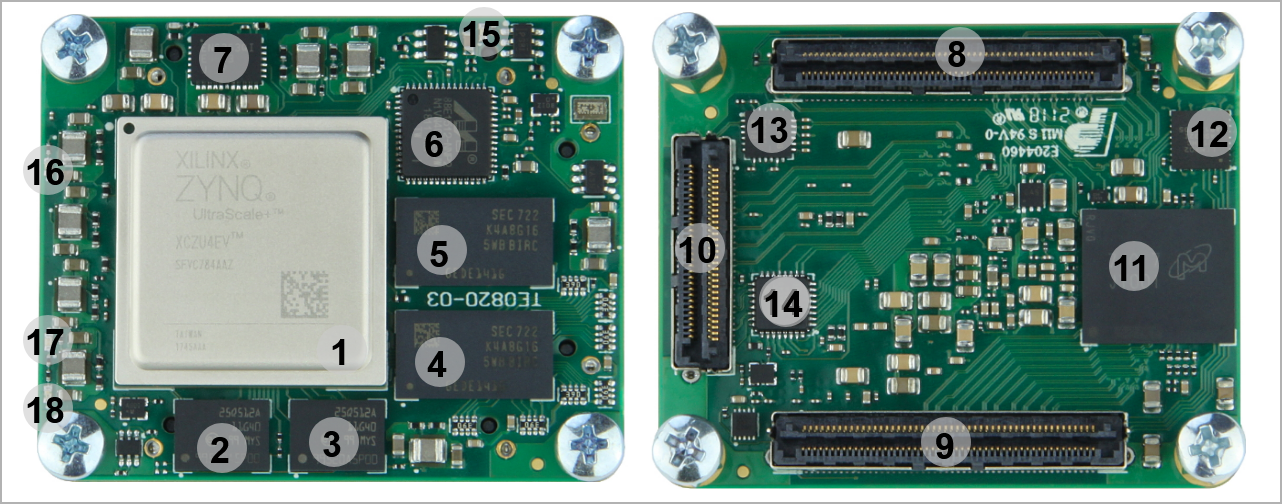
Photo shows similar TE0841-01
- Xilinx Zynq UltraScale+ MPSoC, U1
- 1.8V, 512 Mbit QSPI flash memory, U7
- 1.8V, 512 Mbit QSPI flash memory, U17
- 8 Gbit (512 x 16) DDR4 SDRAM, U2
- 8 Gbit (512 x 16) DDR4 SDRAM, U3
- Marvell Alaska 88E1512 integrated 10/100/1000 Mbps energy efficient ethernet transceiver, U8
- 6A PowerSoC DC-DC converter (PL_VCCINT, 0.85V), U5
- B2B connector Samtec Razor Beam™ LSHM-150, JM1
- B2B connector Samtec Razor Beam™ LSHM-150, JM2
- B2B connector Samtec Razor Beam™ LSHM-130, JM3
- 4 GByte eMMC memory, U6
- Lattice Semiconductor MachXO2 System Controller CPLD, U21
- I2C programmable, any frequency , any output quad clock generator, U10
- Highly integrated full featured hi-speed USB 2.0 ULPItransceiver, U18
Initial Delivery State
| Storage Device Name | Content | Notes |
|---|---|---|
SPI Flash OTP Area | Empty, not programmed | Except serial number programmed by flash vendor. |
SPI Flash Quad Enable bit | Programmed | - |
SPI Flash main array | Not programmed | - |
eFUSE USER | Not programmed | - |
eFUSE Security | Not programmed | - |
| Si5338 OTP NVM | Not programmed | - |
| CPLD (LCMXO2-256HC) | SC0820-02 QSPI Firmware | See Boot Process section |
Table 1: Initial delivery state of programmable devices on the module
...
Two different firmware versions are available, one with the QSPI boot option and other with the SD Card boot option.
| B2B JM1 MODE Pin | QSPI Firmware Version | SD Card Firmware Version |
|---|---|---|
| Low | JTAG | Boot from SD Card |
| High | Boot from Flash | JTAG |
Table 2: Boot mode pin description
...
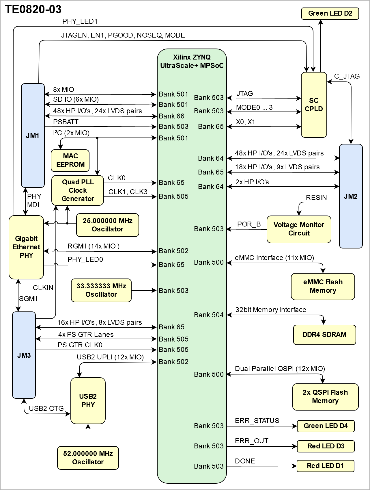
Zynq MPSoC's I/O banks signals connected to the B2B connectors:
| Bank | Type | B2B Connector | I/O Signal Count | Voltage | Notes |
|---|---|---|---|---|---|
64 | HP | JM2 | 48 | User | Max voltage 1.8V |
64 | HP | JM2 | 2 | User | Max voltage 1.8V |
| 65 | HP | JM2 | 18 | User | Max voltage 1.8V |
65 | HP | JM3 | 16 | User | Max voltage 1.8V |
66 | HP | JM1 | 48 | User | Max voltage 1.8V |
501 | MIO | JM1 | 6 | 3.3V | - |
505 | GTR | JM3 | 4 lanes | - | - |
505 | GTR CLK | JM3 | 1 differential input | - | - |
Table 3: General overview of board to board I/O signals
...
The Xilinx Zynq UltraScale+ device used on the TE0820 module has 4 GTR transceivers. All 4 are wired directly to B2B connector JM3. MGT (Multi Gigabit Transceiver) lane consists of one transmit and one receive (TX/RX) differential pairs, four signals total per one MGT lane. Following table lists lane number, FPGA bank number, transceiver type, signal schematic name, board-to-board pin connection and FPGA pins connection:
| Lane | Bank | Type | Signal Name | B2B Pin | FPGA Pin |
|---|---|---|---|---|---|
| 0 | 505 | GTR |
|
|
|
| 1 | 505 | GTR |
|
|
|
| 2 | 505 | GTR |
|
|
|
| 3 | 505 | GTR |
|
|
|
Table 4: MGT lanes
There are 3 clock sources for the GTR transceivers. B505_CLK0 is connected directly to B2B connector JM3, so the clock can be provided by the carrier board. Clocks B505_CLK1 and B505_CLK3 are provided by the on-board clock generator (U10). As there are no capacitive coupling of the data and clock lines that are connected to the connectors, these may be required on the user’s PCB depending on the application.
| Clock signal | Bank | Source | FPGA Pin | Notes |
|---|---|---|---|---|
| B505_CLK0_P | 505 | B2B, JM3-31 | PS_MGTREFCLK0P_505, F23 | Supplied by the carrier board |
| B505_CLK0_N | 505 | B2B, JM3-33 | PS_MGTREFCLK0N_505, F24 | Supplied by the carrier board |
| B505_CLK1_P | 505 | U10, CLK2A | PS_MGTREFCLK1P_505, E21 | On-board Si5338A |
| B505_CLK1_N | 505 | U10, CLK2B | PS_MGTREFCLK1N_505, E22 | On-board Si5338A |
| B505_CLK2_P | 505 | N/A | PS_MGTREFCLK2P_505, C21 | Not connected |
| B505_CLK2_N | 505 | N/A | PS_MGTREFCLK2N_505, C22 | Not connected |
| B505_CLK3_P | 505 | U10, CLK1A | PS_MGTREFCLK3P_505, A21 | On-board Si5338A |
| B505_CLK3_N | 505 | U10, CLK1B | PS_MGTREFCLK3N_505, A22 | On-board Si5338A |
Table 5: MGT reference clock sources
...
JTAG access to the Xilinx Zynq-7000 is provided through B2B connector JM2.
JTAG Signal | B2B Connector Pin |
|---|---|
| TMS | JM2-93 |
| TDI | JM2-95 |
| TDO | JM2-97 |
| TCK | JM2-99 |
Table 6: JTAG interface signals
...
Special purpose pins are connected to System Controller CPLD and have following default configuration:
| Pin Name | Mode | Function | Default Configuration |
|---|---|---|---|
| EN1 | Input | Power Enable | No hard wired function on PCB. When forced low, pulls up PGOOD, goes low without effect on power management. |
| PGOOD | Output | Power Good | Active high when all on-module power supplies are working properly. |
| NOSEQ | - | - | No function. |
| RESIN | Input | Reset | Active low reset, gated to POR_B. |
| JTAGEN | Input | JTAG Select | Low for normal operation, high for CPLD JTAG access. |
Table 7: System Controller CPLD special purpose pins.
See also TE0820-REV01_REV02 CPLD
Default PS MIO Mapping
| PS MIO | Function | B2B Pin | Connected to | PS MIO | Function | B2B Pin | Connected to |
|---|---|---|---|---|---|---|---|
| 0 | SPI0 | - | U7-B2, CLK | 40..45 | - | - | Not connected |
| 1 | SPI0 | - | U7-D2, DO/IO1 | 46 | SD | JM1-17 | B2B, SD_DAT3 |
| 2 | SPI0 | - | U7-C4, WP/IO2 | 47 | SD | JM1-19 | B2B, SD_DAT2 |
| 3 | SPI0 | - | U7-D4, HOLD/IO3 | 48 | SD | JM1-21 | B2B, SD_DAT1 |
| 4 | SPI0 | - | U7-D3, DI/IO0 | 49 | SD | JM1-23 | B2B, SD_DAT0 |
| 5 | SPI0 | - | U7-C2, CS | 50 | SD | JM1-25 | B2B, SD_CMD |
| 6 | N/A | - | Not connected | 51 | SD | JM1-27 | B2B, SD_CLK |
| 7 | SPI1 | - | U17-C2, CS | 52 | USB_PHY | - | U18-31, OTG-DIR |
| 8 | SPI1 | - | U17-D3, DI/IO0 | 53 | USB_PHY | - | U18-31, OTG-DIR |
| 9 | SPI1 | - | U17-D2, DO/IO1 | 54 | USB_PHY | - | U18-5, OTG-DATA2 |
| 10 | SPI1 | - | U17-C4, WP/IO2 | 55 | USB_PHY | - | U18-2, OTG-NXT |
| 11 | SPI1 | - | U17-D4, HOLD/IO3 | 56 | USB_PHY | - | U18-3, OTG-DATA0 |
| 12 | SPI1 | - | U17-B2, CLK | 57 | USB_PHY | - | U18-4, OTG-DATA1 |
| 13..20 | eMMC | - | U6, MMC-D0..D7 | 58 | USB_PHY | - | U18-29, OTG-STP |
| 21 | eMMC | - | U6, MMC-CMD | 59 | USB_PHY | - | U18-6, OTG-DATA3 |
| 22 | eMMC | - | U6, MMC-CLKR | 60 | USB_PHY | - | U18-7, OTG-DATA4 |
| 23 | eMMC | - | U6, MMC-RST | 61 | USB_PHY | - | U18-9, OTG-DATA5 |
| 24 | ETH | - | U8, ETH-RST | 62 | USB_PHY | - | U18-10, OTG-DATA6 |
| 25 | USB_PHY | - | U18, OTG-RST | 63 | USB_PHY | - | U18-13, OTG-DATA7 |
| 26 | MIO | JM1-95 | B2B, as PJTAG MIO possible | 64 | ETH | - | U8-53, ETH-TXCK |
| 27 | MIO | JM1-93 | B2B, as PJTAG MIO possible | 65..66 | ETH | - | U8-50..51, ETH-TXD0..1 |
| 28 | MIO | JM1-99 | B2B, as PJTAG MIO possible | 67..68 | ETH | - | U8-54..55, ETH-TXD2..3 |
| 29 | MIO | JM1-99 | B2B, as PJTAG MIO possible | 69 | ETH | - | U8-56, ETH-TXCTL |
| 30 | MIO | JM1-92 | B2B (UART RX) | 70 | ETH | - | U8-46, ETH-RXCK |
| 31 | MIO | JM1-85 | B2B (UART TX) | 71..72 | ETH | - | U8-44..45, ETH-RXD0..1 |
| 32 | MIO | JM1-91 | B2B | 73..74 | ETH | - | U8-47..48, ETH-RXD2..3 |
| 33 | MIO | JM1-87 | B2B | 75 | ETH | - | U8-43, ETH-RXCTL |
| 34..37 | - | - | Not connected | 76 | ETH | - | U8-7, ETH-MDC |
| 38 | I2C | - | U10-12, SCL | 77 | ETH | - | U8-8, ETH-MDIO |
| 39 | I2C | - | U10-19, SDA | - | - | - | - |
Table 8: TE0820-02 PS MIO mapping
...
On-board Gigabit Ethernet PHY is provided with Marvell Alaska 88E1512 chip. The Ethernet PHY RGMII interface is connected to the Zynq Ethernet0 PS GEM0. I/O voltage is fixed at 1.8V for HSTL signaling. SGMII (SFP copper or fiber) can be used directly with the Ethernet PHY, as the SGMII pins are available on the B2B connector JM3. The reference clock input of the PHY is supplied from an on-board 25MHz oscillator (U11), the 125MHz output clock is left unconnected.
Ethernet PHY connection
| PHY Pin | ZYNQ PS | ZYNQ PL | Notes |
|---|---|---|---|
| MDC/MDIO | MIO76, MIO77 | - | - |
| LED0 | - | K8 | Can be routed via PL to any free PL I/O pin in B2B connector. |
| LED1 | - | - | CPLD pin 17. |
| LED2 | - | - | Not connected. |
| CONFIG | - | - | Wired to the 1.8V. |
| RESETn | MIO24 | - | - |
| RGMII | MIO64..MIO75 | - | - |
| SGMII | - | - | Routed to the B2B connector JM3. |
Table 9: General overview of the Gigabit Ethernet PHY signals
...
USB PHY is provided by Microchip USB3320. The ULPI interface is connected to the Zynq PS USB0. I/O voltage is fixed at 1.8V. Reference clock input for the USB PHY is supplied by the on-board 25.000000 MHz oscillator (U15).
USB PHY connection
| PHY Pin | ZYNQ Pin | B2B Name | Notes |
|---|---|---|---|
| ULPI | MIO52..63 | - | Zynq USB0 MIO pins are connected to the USB PHY. |
| REFCLK | - | - | 52.000000 MHz from on-board oscillator (U14). |
| REFSEL[0..2] | - | - | Reference clock frequency select, all set to GND selects 52.000000 MHz. |
| RESETB | MIO25 | - | Active low reset. |
| CLKOUT | MIO52 | - | Connected to 1.8V, selects reference clock operation mode. |
| DP, DM | - | OTG_D_P, OTG_D_N | USB data lines routed to B2B connector JM3 pins 47 and 49. |
| CPEN | - | VBUS_V_EN | External USB power switch active high enable signal, routed to JM3 pin 17. |
| VBUS | - | USB_VBUS | Connect to USB VBUS via a series of resistors, see reference schematics, routed to JM3 pin 55. |
| ID | - | OTG_ID | For an A-device connect to ground, for a B-device left floating. routed from JM3 pin 23. |
Table 10: General overview of the USB PHY signals.
...
On-board I2C devices are connected to MIO38 (SCL) and MIO39 (SDA) which are configured as I2C1 by default. Addresses for on-board I2C slave devices are listed in the table below:
| I2C Device | I2C Address | Notes |
|---|---|---|
Si5338A PLL | 0x70 | - |
| EEPROM | 0x53 | - |
Table 11: Address table of the I2C bus slave devices.
...
Once running, the frequency and other parameters can be changed by programming the device using the I2C bus connected between the FPGA (master) and clock generator (slave). For this, proper I2C bus logic has to be implemented in FPGA.
| Signal | Frequency | Notes |
|---|---|---|
| IN1/IN2 | - | Not used (external clock signal supply). |
IN3 | 25.000000 MHz | Fixed input clock signal from reference clock generator SiT8008BI-73-18S-25.000000E (U11). |
| IN4 | - | LSB of the default I2C address, wired to ground mean address is 0x70. |
IN5 | - | Not connected. |
IN6 | - | Wired to ground. |
| CLK0 A/B | - | Bank 65 clock input, pins K9 and J9. |
CLK1 A/B | - | MGT reference clock 3 to FPGA Bank 505 MGT. |
CLK2 A/B | - | MGT reference clock 1 to FPGA Bank 505 MGT. |
| CLK3 A/B | - | Not connected. |
Table 12: General overview of the on-board quad clock generator I/O signals
...
The module has following reference clock signals provided by on-board oscillators and external source from carrier board:
| Clock Source | Schematic Name | Frequency | Clock Destination |
|---|---|---|---|
| SiTime SiT8008BI oscillator, U21 | PS_CLK | 33.333333 MHz | Zynq MPSoC U1,pin R16 |
| SiTime SiT8008BI oscillator, U21 | - | 25.000000 MHz | Quad PLL clock generator U10, pin 3, and Ethernet PHY U8, pin 34 |
Table 13: Reference clock signals
On-board LEDs
| LED | Color | Connected to | Description and Notes |
|---|---|---|---|
| D1 | Red | PS Config bank 503 | Reflects inverted DONE signal when FPGA configuration is completed |
| D2 | Green | System Controller CPLD, bank 3 | Exact function is defined by SC CPLD firmware |
| D3 | Red | PS Config bank 503 | Reflects Zynq MPSoC control signal 'ERR_OUT' |
| D4 | Green | PS Config bank 503 | Reflects Zynq MPSoC control signal 'ERR_STATUS' |
Table 14: On-board LEDs
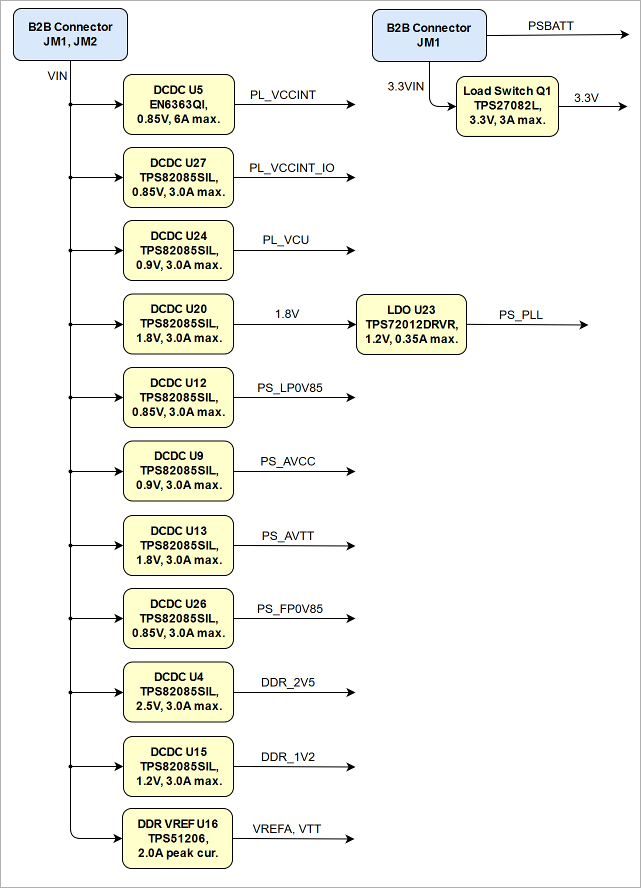
Power and Power-on Sequence
...
Power supply with minimum current capability of 3A for system startup is recommended.
Power Consumption
| Power Input | Typical Current |
|---|---|
| VIN | TBD* |
| 3.3VIN | TBD* |
Table 15: Power consumption
...
| Warning |
|---|
| To avoid any damage to the module, check for stabilized on-board voltages should be carried out (i.e. power good and enable signals) before powering up any FPGAZynq's I/O bank voltages VCCO_x. All I/Os should be tri-stated during power-on sequence. |
...
| Scroll Title | ||||||||||||||||||||||||||||||||||
|---|---|---|---|---|---|---|---|---|---|---|---|---|---|---|---|---|---|---|---|---|---|---|---|---|---|---|---|---|---|---|---|---|---|---|
| ||||||||||||||||||||||||||||||||||
|
See also Xilinx datasheet DS892 DS925 for additional information. User should also check related base board documentation when intending base board design for TE0841 TE0820 module.
Power-On Sequence
The TE0820 SoM meets the recommended criteria to power up the Xilinx Zynq chip properly by keeping a specific sequence of enabling the on-board DC-DC converters dedicated to the particular functional units of the Zynq chip and powering up the on-board voltages.
...
| Scroll Title | ||||||||||||||||||||||||||||||||||
|---|---|---|---|---|---|---|---|---|---|---|---|---|---|---|---|---|---|---|---|---|---|---|---|---|---|---|---|---|---|---|---|---|---|---|
| ||||||||||||||||||||||||||||||||||
|
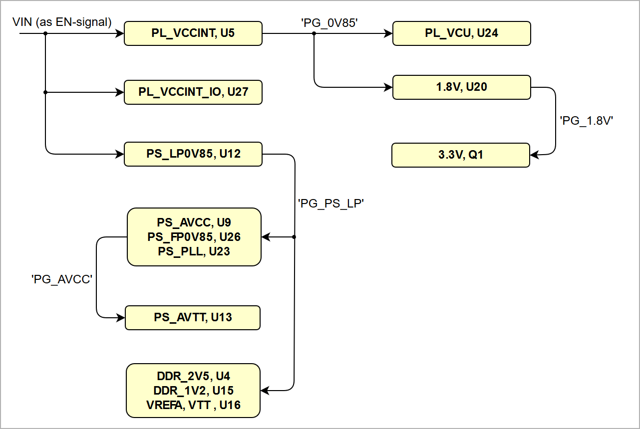
Figure 4: TE0820-03 power-on sequence diagram.
...
See Xilinx datasheet DS925 for additional information. User should also check related carrier board documentation when choosing carrier board design for TE0715 module.
Power Rails
| Power Rail Name on B2B Connector | JM1 Pins | JM2 Pins | Direction | Notes |
|---|---|---|---|---|
| VIN | 1, 3, 5 | 2, 4, 6, 8 | Input | Supply voltage from the carrier board. |
| 3.3V | - | 10, 12 | Output | Internal 3.3V voltage level. |
| 3.3VIN | 13, 15 | - | Input | Supply voltage from the carrier board. |
| 1.8V | 39 | - | Output | Internal 1.8V voltage level. |
| JTAG VREF | - | 91 | Output | JTAG reference voltage. Attention: Net name on schematic is "3.3VIN" |
| VCCO_64 | - | 7, 9 | Input | High performance I/O bank voltage. |
| VCCO_65 | - | 5 | Input | High performance I/O bank voltage. |
| VCCO_66 | 9, 11 | - | Input | High performance I/O bank voltage. |
Table 16: TE0820-02 power rails
Bank Voltages
| Bank | Name on Schematic | Voltage | Range |
|---|---|---|---|
| 64 HP | VCCO_64 | User | HP: 1.0V to 1.8V |
| 65 HP | VCCO_65 | User | HP: 1.0V to 1.8V |
| 66 HP | VCCO_66 | User | HP: 1.0V to 1.8V |
| 500 PSMIO | VCCO_PSIO0_500 | 1.8V | - |
| 501 PSMIO | VCCO_PSIO1_501 | 3.3V | - |
| 502 PSMIO | VCCO_PSIO2_502 | 1.8V | - |
| 503 PSCONFIG | VCCO_PSIO3_503 | 1.8V | - |
| 504 PSDDR | VCCO_PSDDR_504 | 1.2V | - |
Table 17: TE0820-02 I/O bank voltages
...
Variants Currently In Production
| Trenz shop TE0820 overview page | |
|---|---|
| English page | German page |
Technical Specifications
Absolute Maximum Ratings
Parameter | Min | Max | Units | Notes |
|---|---|---|---|---|
VIN supply voltage | -0.3 | 7 | V | See EN6347QI and TPS82085SIL datasheets |
| 3.3VIN supply voltage | -0.1 | 3.630 | V | Xilinx DS925 and TPS27082L datasheet |
| PS I/O supply voltage, VCCO_PSIO | -0.5 | 3.630 | V | Xilinx document DS925 |
| PS I/O input voltage | -0.5 | VCCO_PSIO + 0.55 | V | Xilinx document DS925 |
| HP I/O bank supply voltage, VCCO | -0.5 | 2.0 | V | Xilinx document DS925 |
| HP I/O bank input voltage | -0.55 | VCCO + 0.55 | V | Xilinx document DS925 |
Voltage on SC CPLD pins | -0.5 | 3.75 | V | Lattice Semiconductor MachXO2 datasheet |
Storage temperature | -40 | +85 | °C | See eMMC datasheet |
Table 18: Module absolute maximum ratings
Recommended Operating Conditions
| Parameter | Min | Max | Units | Notes |
|---|---|---|---|---|
| VIN supply voltage | 2.5 | 6 | V | See TPS82085S datasheet |
| 3.3VIN supply voltage | 2.375 | 3.465 | V | See LCMXO2-256HC, Xilinx DS925 datasheet |
| PS I/O supply voltage, VCCO_PSIO | 1.710 | 3.465 | V | Xilinx document DS925 |
| PS I/O input voltage | –0.20 | VCCO_PSIO + 0.20 | V | Xilinx document DS925 |
| HP I/O banks supply voltage, VCCO | 0.950 | 1.9 | V | Xilinx document DS925 |
| HP I/O banks input voltage | -0.20 | VCCO + 0.20 | V | Xilinx document DS925 |
| Voltage on SC CPLD pins | -0.3 | 3.6 | V | Lattice Semiconductor MachXO2 datasheet |
Table 19: Recommended operating conditions
...
Hardware Revision History
| Date | Revision | Notes | PCN Link | Documentation Link |
|---|---|---|---|---|
| - | 03 | current available module revision | - | TE0820-03 |
| 2017-08-17 | 02 | -- | PCN-20171117 | TE0820-02 |
| 2016-12-23 | 01 | Prototype only | - | TE0820-01 |
Table 20: Hardware revision history table.
...
| HTML |
|---|
<!-- Generate new entry: 1.add new row below first 2.Copy "Page Information Macro(date)" Macro-Preview, Metadata Version number, Author Name and description to the empty row. Important Revision number must be the same as the Wiki document revision number 3.Update Metadata = "Page Information Macro (current-version)" Preview+1 and add Author and change description. --> |
Date | Revision | Contributors | Description | ||||||||||||||||||||||||
|---|---|---|---|---|---|---|---|---|---|---|---|---|---|---|---|---|---|---|---|---|---|---|---|---|---|---|---|
|
|
|
| ||||||||||||||||||||||||
| v.61 | John Hartfiel |
| |||||||||||||||||||||||||
| 2018-03-12 | v.54 |
| |||||||||||||||||||||||||
| 2017-11-20 | v.51 | John Hartfiel |
| ||||||||||||||||||||||||
| 2017-11-10 | v.50 | John Hartfiel |
| ||||||||||||||||||||||||
| 2017-10-18 | v.49 | John Hartfiel |
| ||||||||||||||||||||||||
| 2017-09-25 | v.48 | John Hartfiel |
| ||||||||||||||||||||||||
| 2017-09-18 | v.47 | John Hartfiel |
| ||||||||||||||||||||||||
| 2017-08-30 | v.46 | Jan Kumann |
| ||||||||||||||||||||||||
2017-08-24 | v.36 | John Hartfiel |
| ||||||||||||||||||||||||
| 2017-08-21 | v.34 | John Hartfiel |
| ||||||||||||||||||||||||
| 2017-08-21 | v.33 | Jan Kumann |
| ||||||||||||||||||||||||
| v.7 | John Hartfiel |
| ||||||||||||||||||||||||
2017-08-07 | v.5 | Jan Kumann | Initial version. |
Table 21: Document change history
...
Overview
Content Tools