Page History
...
| Pin Name | Direction | Function | Default Configuration | |
|---|---|---|---|---|
| EXT_IO1 ... EXT_IO40 | in / out | user GPIO on B2B | see current CPLD firmware | |
| BOOTMODE | in | in | signal forwarded to MIO9 and currently used as UART RX line | |
| CONFIGX | in | out | signal forwarded to MIO8 and currently used as UART TX line | |
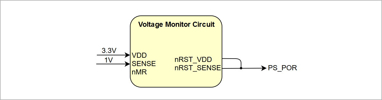
| NRST_IN | in | nRESET input | external Board Reset | |
| M_TDO | out | CPLD JTAG interface | - | |
| M_TDI | in | |||
| M_TCK | in | |||
| M_TMS | in | |||
| JTAGENB | in | enable JTAG | pull high for programming SC CPLD firmware | |
| ETH1_RESET | out | reset GbE PHY U18 | see current SC CPLD firmware | |
| OTG-RST | out | reset USB2 PHYs U4 and U8 | see current SC CPLD firmware | |
| DONE | in | Zynq control signal | PL configuration completed | |
| PROG_B | out | PL configuration reset signal | ||
| PS_POR | out | PS power-on reset | ||
| BM2/MIO4 | out | Bootmode Pin: SD or QSPI | ||
| MIO14 | in | user MIO pins | currently used as UART interface | |
| MIO15 | out | |||
| LED2 | out | Red LED D1 status signal | see current CPLD firmware | |
| CPLD_GPIO0 ... CPLD_GPIO3 | in / out | user GPIO on B2B | CPLD_GPIO3 used for Boot Mode | see current CPLD firmware |
| FPGA_CPLD1 ... FPGA_CPLD4 | in /out | user GPIO to FPGA bank 9 | see current SC CPLD firmware | |
| EN_1V | out | Power control | enable signal DCDC U13 '1V' | |
| PG_ALL | in | power good signal all voltages powered up properly → Green LED D2 lights up. |
...
| Scroll Title | ||||||||||||||||||||||||
|---|---|---|---|---|---|---|---|---|---|---|---|---|---|---|---|---|---|---|---|---|---|---|---|---|
| ||||||||||||||||||||||||
|
Power Rails
| Power Rail Name on B2B Connector | J1 Pins | J2 Pins | J3 Pins | Direction | Notes |
|---|---|---|---|---|---|
| VIN | - | 165, 166, 167, 168 | - | Input | external power supply voltage |
| C3.3V | - | 147, 148 | - | Input | Normally leave unconnected |
| 3.3V | - | 111, 112, 123, 124, 135 136 169, 170, 171, 172 | - | Output | internal 3.3V voltage level |
| 1.8V | 169, 170, 171, 172 | - | - | Output | internal 1.8V voltage level |
| EXT_IO_VCC | 99, 100 | - | - | Input | SC CPLD bank 1, 2 and 4 voltage |
| VCCIO_10 | - | - | 99, 100 | Input | high range I/O bank voltage |
| VCCIO_11 | - | - | 159, 160 | Input | high range I/O bank voltage |
| VCCIO_12 | - | 159, 160 | - | Input | high range I/O bank voltage |
| VCCIO_13 | - | 99, 100 | - | Input | high range I/O bank voltage |
| VBAT_IN | - | - | 124 | Input | backup battery voltage |
...
| Scroll Title | ||||
|---|---|---|---|---|
| ||||
|
...
| Scroll Title | ||||
|---|---|---|---|---|
| ||||
|
...
Overview
Content Tools