Page History
...
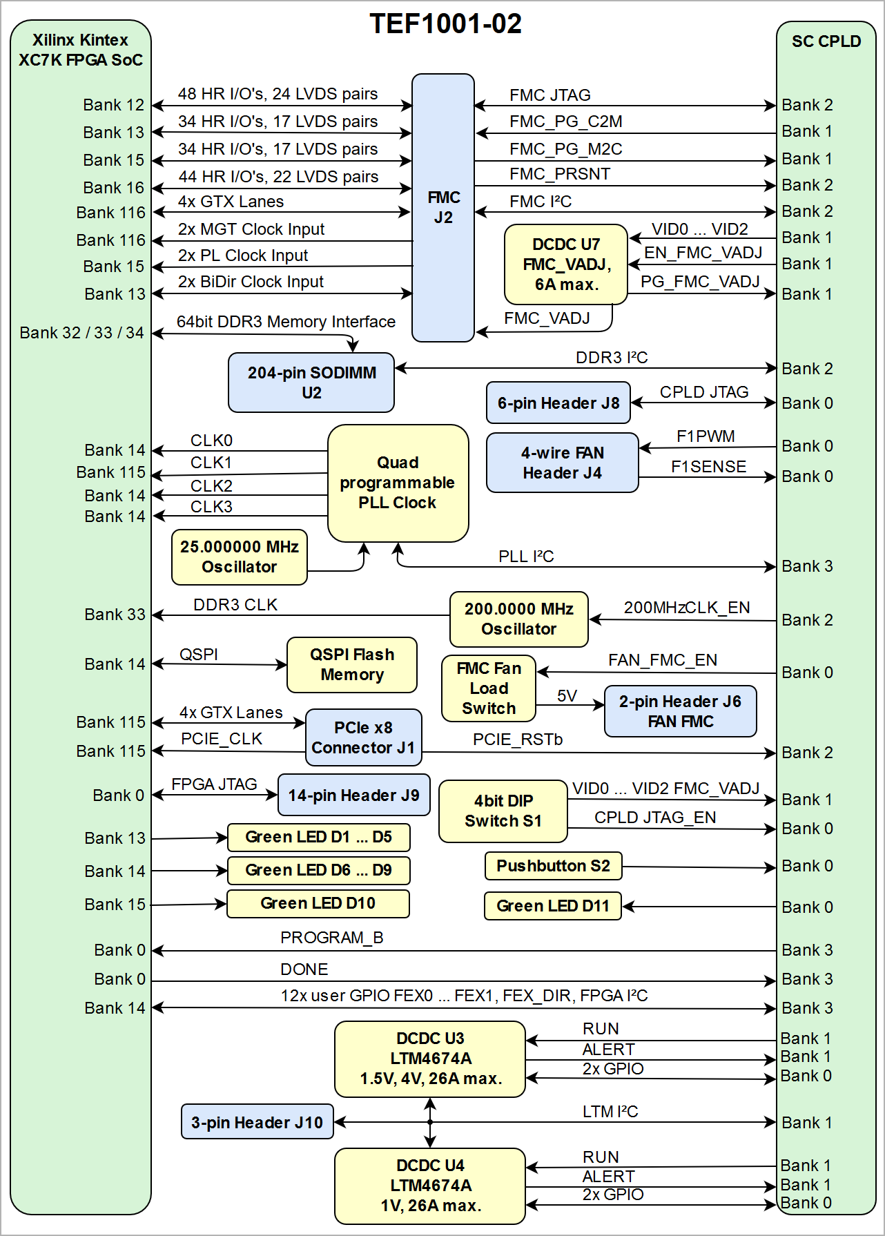
The Trenz Electronic TEF1001 FPGA board is a PCI Express form factor card (PCIe 2.0 or higher) integrating the Xilinx Kintex-7 XC7K160T, XC7K325T or XC7K410T FPGA SoC. The FPGA-board is designed for high system resources and intended for use in applications with high demands on system performance and throughput. The board offers a SO-DIMM socket on the board for standard DDR3 SDRAM extension memory moduleTo extent the board with standard DDR3 SDRAM memory module, there is a 204-pin SODIMM socket with 64bit databus width on the board present.
The board offers a HPC (High Pin Count) ANSI/VITA 57.1 compatible FMC interface connector for standard FPGA Mezzanine cards and modules. Other interface connectors found on-board include JTAG for accessing FPGA and on-board System Controller CPLD, and also connector with 5 high-speed I/O differential signaling pairs.
...
| Scroll Title | ||||||||||||||||||||||||||||||||
|---|---|---|---|---|---|---|---|---|---|---|---|---|---|---|---|---|---|---|---|---|---|---|---|---|---|---|---|---|---|---|---|---|
| ||||||||||||||||||||||||||||||||
|
...
| Scroll Title | ||||||||||||||||||||||||||||||||
|---|---|---|---|---|---|---|---|---|---|---|---|---|---|---|---|---|---|---|---|---|---|---|---|---|---|---|---|---|---|---|---|---|
| ||||||||||||||||||||||||||||||||
|
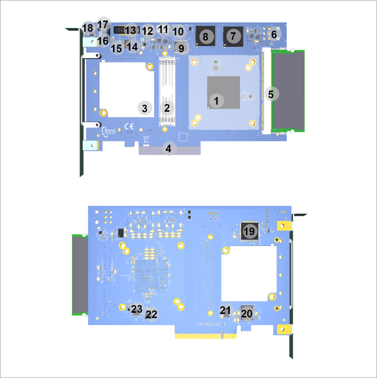
- Xilinx Kintex XC7K-2FBG676I FPGA SoC, U6
- ANSI/VITA 57.1 compliant FMC HPC connector, J2
- Cooling fan 5VDC M1 (45X5MM, 0.7W, 1.06CFM), M1
- PCIe x8 connector, J1
- SO-DIMM socket, U2
- 6-pin 12V power connector, J5
- Step-down DC-DC converter @1.5V and @4V (LT LTM4676A), U3
- Step-down DC-DC converter @1.0V (LT LTM4676A), U4
- 256 Mbit Quad SPI Flash Memory (Micron N25Q256A), U12
- 10x Green user LEDs, D1 ... D10
- 4-wire PWM fan connector, J4
- User button, S2
- FPGA JTAG connector, J9
- sd
- sd
- sd
- sd
- s
- sd
- sd
- s
- sd
- sd
- s
- s
- sd
- sd
- sd
- sd
- FPGA JTAG connector, J9
- User button, S2
- SO-DIMM socket, U2
- Xilinx Virtex-7 XC7VX330T-2FFG1157C FPGA, U1
- ANSI/VITA 57.1 compliant FMC HPC connector, J2
- SMA coaxial connector for external clock input, J3
- System Controller CPLD JTAG connector, J8
- I2C connector for LT LTM4676 step-down DC-DC regulator, J10
- IDC header for access to 5 x high-speed data lanes (LVDS pairs), J7
- 4-wire PWM fan connector, J4
- 6-pin 12V power connector, J5
- Reference clock generator @10.0 MHz (P5146) , U11
- LDO DC-DC regulator @3.3V (LMK_3V3) (TI TPS74901RGWR), U21
- 256 Mbit Quad SPI Flash Memory (Micron N25Q256A), U12
- Cooling fan 5VDC M1 (45X5MM, 0.7W, 1.06CFM)
- System Controller CPLD (Lattice Semiconductor LCMXO2-1200HC), U5
- Ultra low jitter clock synthesizer (TI LMK04828B), U9
- Step-down DC-DC regulator @1.0V (LT LTM4676), U4
- Step-down DC-DC regulator @1.5V (VCC1V5) (LT LTM4676, U3
- I2C Programmable quad clock generator (Silicon Labs Si5338A), U13
- 4A PowerSoC DC-DC converter @1.8V (Altera EN6347QI, U20
- LDO DC-DC regulator @1.0V (MGTAVCC_FPGA) (TI TPS74401RGW), U18
- LDO DC-DC regulator @1.2V (MGTAVTT_FPGA) (TI TPS74401RGW), U17
- 4A PowerSoC DC-DC converter @3.3V (3V3FMC) (Altera EN6347QI), U15
- 4A PowerSoC DC-DC converter @1.8V (FMC_VADJ) (Altera EN6347QI), U7
Initial Delivery State
| Storage device name | Content | Notes |
|---|---|---|
| 24LC128-I/ST | not programmed | User content |
24AA025E48 EEPROM's | User content not programmed | Valid MAC Address from manufacturer |
| Si5338A OTP Area | not programmed | - |
| eMMC Flash Memory | Empty, not programmed | Except serial number programmed by flash vendor |
SPI Flash OTP Area | Empty, not programmed | Except serial number programmed by flash vendor |
SPI Flash Quad Enable bit | Programmed | - |
SPI Flash main array | demo design | - |
| HyperFlash Memory | not programmed | - |
eFUSE USER | Not programmed | - |
eFUSE Security | Not programmed | - |
...
Overview
Content Tools