Page History
...
The TEF1001 FPGA board is a PCI Express card designed to fit into systems with PCI Express x8 slots and has a data transmission capability which meets PCIe Gen. 2 with 4 GTX lanes connected to the PCIe interface.
See next section for the overview of FPGA MGT lanes routed to the PCIe interface.
...
Table below describes the functionalities of the switches of DIP-switches S3 and S4 at their each positions:
| DIP-switch S3 | Signal Schematic Name | Connected to | Functionality | Notes |
|---|---|---|---|---|
| S1-1 | JTAG_EN | SC CPLD U5, bank 1, pin 82 | enables JTAG interface of SC CPLD U5 | SC CPLD programmable through JTAG connector, J8 |
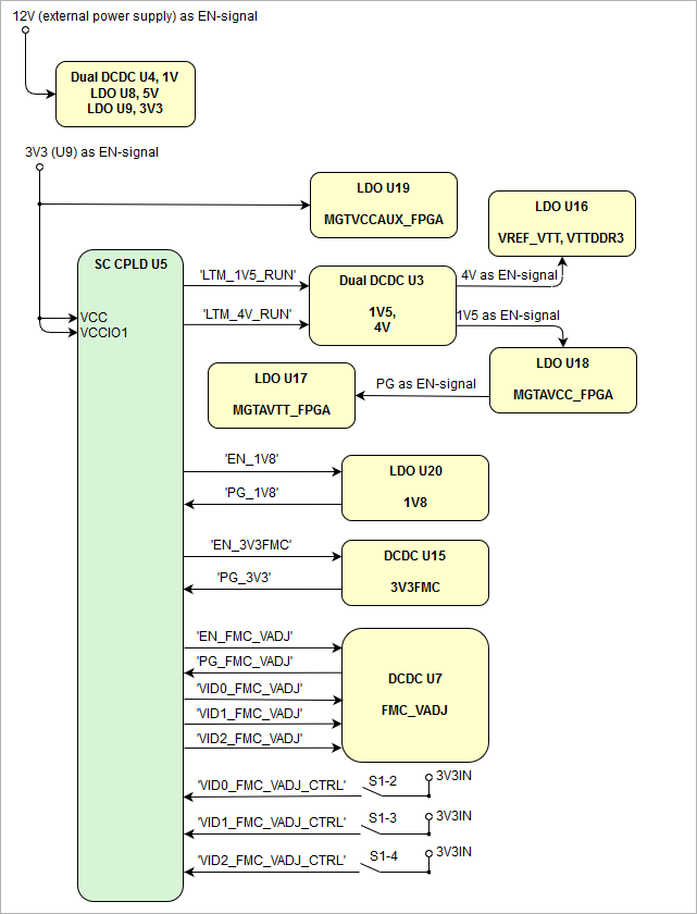
| S1-2 | VID0_FMC_VADJ_CTRL | SC CPLD U5, bank 1, pin 71 | set 3-bit code to set FMC_VADJ voltage | The FMC_VADJ voltage is provided by DCDC U7 EN5365QI, the voltage can be set from 0.8V to 3.3V in 7 steps, see |
| S1-3 | VID1_FMC_VADJ_CTRL | SC CPLD U5, bank 1, pin 63 | ||
| S1-4 | VID2_FMC_VADJ_CTRL | SC CPLD U5, bank 1, pin 62 |
Table 13: DIP-switch S1 functionality description
...
| Scroll Title | ||||||||||||||||||||||||||||||||
|---|---|---|---|---|---|---|---|---|---|---|---|---|---|---|---|---|---|---|---|---|---|---|---|---|---|---|---|---|---|---|---|---|
| ||||||||||||||||||||||||||||||||
|
...
Bank Voltages
| Bank | Schematic Name | Voltage | Range | Notes |
|---|---|---|---|---|
| 0 | 1V8 | 1.8V |
| - | Config bank |
| 0 fixed to 1.8V |
| 12 |
| FMC_VADJ | user | HR |
| : 1.2V to |
| 3. |
| 3V | FMC_VADJ voltage ajustable by DIP switch S1 | ||
| 13 | FMC_VADJ | user | HR |
| : 1.2V |
| to 3. |
| 3V | FMC_VADJ voltage ajustable by DIP switch S1 |
| 14 |
| 1V8 | 1.8V |
| HR: 1.2V to 3.3V | PL bank 14 fixed to 1.8V |
| 15 | FMC_VADJ | user | HR |
| : 1.2V |
| to 3. |
| 3V | FMC_VADJ voltage ajustable by DIP switch S1 | ||
| 16 | VIO_B_FMC | user | HR |
| : 1.2V to 3.3V | PL bank 16 fixed to 1.8V |
| 32 | 1V5 | 1.5V | HP: 1.2V to 1.8V | DDR3 memory interface |
| 33 |
| 1V5 | 1.5V | HP: 1.2V to 1.8V | DDR3 memory interface |
| 34 |
| 1V5 | 1.5V | HP: 1.2V to 1.8V | DDR3 memory interface |
115 116 |
117
118MGTAVCC_FPGA MGTVCCAUX |
MGTAVTT_FPGA
1.0V
1.8V
1.2V
MGT bank supply voltage
MGT bank auxiliary supply voltage
MGT bank termination circuits voltage
Table 15: Module power rails
...
_FPGA MGTAVTT_FPGA | 1.0V 1.8V 1.2V | MGT bank supply voltage MGT bank auxiliary supply voltage MGT bank termination circuits voltage | MGT banks with Xilinx GTX transceiver units |
Table 15: Board I/O bank voltages
Power Rails
| Connector / Pin | Voltage | Direction | Notes |
|---|---|---|---|
| J4, pin 2 | 12V |
| Output | 4-wire PWM fan connector supply voltage | |
| J6, pin 2 | 5V |
| Output | Cooling fan M1 supply voltage | |
| J8, pin 6 |
| 3V3 | Output | VCCIO CPLD JTAG | |
| J9, pin 2 | 1V8 | Output | VCCIO FPGA JTAG |
| J2, pin C35 / C37 | 12V | Output |
| FMC supply voltage |
| J2, pin D32 |
| 3V3 | Output | VCCIO FMC | |
| J2, pin D36 / D38 / D39 / D40 | 3V3FMC | Output | VCCIO FMC |
| J2, pin H1 | VREF_A_M2C | Input | VREF voltage for bank |
| 13 / |
| 15 | |||
| J2, pin K1 | VREF_B_M2C | Input | VREF voltage for bank |
| 16 | |||
| J2, pin J39 / J40 | VIO_B_FMC | Input | PL I/O voltage bank |
| 16 (VCCO) | |
| J2, pin H40 / G39 / F40 / E39 | FMC_VADJ |
| Output | PL I/O voltage bank 12 / 13 / 15 (VCCO) | |
| J1, pin |
| B1 / B2 / B3 / A2 / A3 | 12V_input_B |
| Input |
| 12V main power supply from PCIe connector | |||
| J5, pin 1 / 2 / 3 | 12V_input_A | Input | Main power supply connector |
Table 16: Module PL I/O bank voltages Board power rails
Variants Currently In Production
...
| Parameter | Min | Max | Units | Reference Document | |||||
|---|---|---|---|---|---|---|---|---|---|
| VIN supply voltage | 11.4 | 12.6 | V | 12V nominal, ANSI/VITA 57.1 power specification for FMC connector | |||||
| Supply voltage for HR I/O banks (VCCO) | 1.140 | 3.465 | V | Xilinx datasheet DS182 | |||||
Supply voltage for HP I/O banks (VCCO) | 1.140 | 1.890 | V | Xilinx datasheet DS182 | |||||
I/O input voltage for HR I/O banks | –0-0.500 | VCCO + 0.20 | V | Xilinx datasheet DS182 | |||||
| I/O input voltage for HP I/O banks | –0-0.500 | VCCO + 0.20 | V | Xilinx datasheet DS182 | |||||
| Differential input voltage | -0.2 | 2.625 | V | Xilinx datasheet DS182 | |||||
| I/O input voltage for SC CPLD U5 | -0.3 | 3.6 | V | Lattice MachXO2 Family datasheet | |||||
| Voltages on LTM4676 I²C pins (LTM_SCL, LTM_SDA), header J10 | 0 | 3.3V | V | LTM4676A datasheet | |||||
Industrial Module Board Operating Temperature Range | -40 | 85 | °C | Xilinx datasheet DS182 | Commercial Module Operating Temperature Range | 0 | 85°C | Xilinx DS182, Silicon Labs Si5338 datasheets |
Table 18: Module recommended operating conditions
...
Board size: 50 mm × 40 mm. Please download the assembly diagram for exact numbers.
PCB thickness: ca. 1.55 mm.
The board meets the PCIe standard specifications for the dimensions of a PCIe cardCard Electromechanical specifications Revision 1.1
All dimensions are given in millimeters.
...
Overview
Content Tools