...
| Scroll Title |
|---|
| anchor | Figure_BD |
|---|
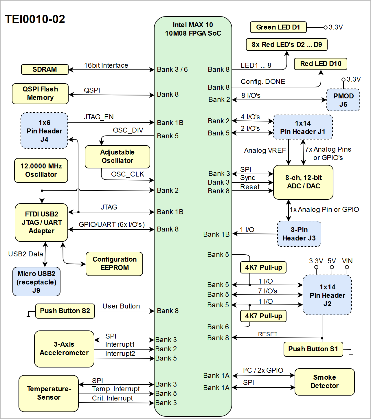
| title | Figure 1: TEI0010 block diagram |
|---|
|
| Scroll Ignore |
|---|
| draw.io Diagram |
|---|
| border | falsetrue |
|---|
| viewerToolbar | true |
|---|
| |
|---|
| fitWindow | false |
|---|
| diagramDisplayName | |
|---|
| lbox | true |
|---|
| revision | 3 |
|---|
| diagramName | TEI0010 block diagram |
|---|
| simpleViewer | false |
|---|
| width | |
|---|
| links | auto |
|---|
| tbstyle | hidden |
|---|
| diagramWidth | 641 |
|---|
|
|
| Scroll Only |
|---|
|
|
...
| Scroll Title |
|---|
| anchor | Table_OV_I/O's |
|---|
| title | General overview of single ended I/O's |
|---|
|
| Scroll Table Layout |
|---|
| orientation | portrait |
|---|
| sortDirection | ASC |
|---|
| repeatTableHeaders | default |
|---|
| style | |
|---|
| widths | |
|---|
| sortByColumn | 1 |
|---|
| sortEnabled | false |
|---|
| cellHighlighting | true |
|---|
|
| Bank | Connector Designator | I/O Signal Count | Bank Voltage | Notes |
|---|
| 2 | J1 | 4 I/O's | 3.3V | - | | J6 | 8 I/O's | Pmod connector | | 5 | J1 | 2 I/O's | 3.3V | - | | J2 | 9 I/O's | 2 I/O's of bank 5 can be pulled-up to 3.3V (4K7 resistors) | | 1B | J4 | JTAG interface and 'JTAGEN' signal (5 I/O's) | 3.3V | JTAG enable signal (JTAGEN) on pin J4-2, switch between user I/O pins and JTAG pin functions | | J3 | 1 I/O | - |
|
FPGA I/O banks
Table below contains the signals and interfaces of the FPGA banks connected to pins and peripherals of the board:
| Scroll Title |
|---|
| anchor | Table_OV_I/O's |
|---|
| title | General overview of single ended I/O's |
|---|
|
| Scroll Table Layout |
|---|
| orientation | portrait |
|---|
| sortDirection | ASC |
|---|
| repeatTableHeaders | default |
|---|
| style | |
|---|
| widths | |
|---|
| sortByColumn | 1 |
|---|
| sortEnabled | false |
|---|
| cellHighlighting | true |
|---|
|
| Bank | I/O's Count | Connected to | Notes |
|---|
| 2 | 4 | 1x14 pin header, J1 | user GPIO's | | 8 | Pmod connector, J6 | user GPIO's | | 1 | clock oscillator, U7 | 12.0000 MHz reference clock input | | 1 | reference clock oscillator, U10 | reference clock input from oscillator U10 | | 1 | accelerometer IC, U11 | interrupt 1 line of Analog Devices MEMS accelerometer | | 5 | 9 | 1x14 pin header, J2 | 2 I/O's (D11, D12) of bank 5 can be pulled-up to 3.3V (4K7 resistors) with 1 I/O (D12_R) of same Bank and 1 I/O (D11_R) of bank 6 | | 1 | accelerometer IC, U11 | interrupt 2 line of Analog Devices MEMS accelerometer | | 1 | reference clock oscillator, U10 | oscillator adjustable with three steps of clock output | | 1 | temperature sensor IC, U8 | interrupt line of temperature thresholds | | 6 | 18 | 8 MByte SDRAM 166MHz, U2 | 16bit SDRAM memory interface | | 3 | 22 | 8 MByte SDRAM 166MHz, U2 | 16bit SDRAM memory interface | | 3 | SPI interface connected to IC U8, U11, U12 | SPI interface (MISO, MOSI, MCLK) for temperature sensor U8, 3-axis accelerometer U11 and ADC/DAC U12 | | 1 | temperature sensor IC, U8 | chip-select line for SPI interface | | 1 | accelerometer IC, U11 | chip-select line for SPI interface | | 1 | ADC/DAC IC , U12 | Synchronization line of ACD/DAC IC (active low control input) | | 1 | temperature sensor IC, U8 | interrupt line of critical temperature | | 1A | 8 | 1x14 pin headers J1 | 7 analog inputs or GPIO's, 1 pin analog reference voltage input | | 2 | pin headers J1 | 1 analog inputs or GPIO, 1 dedicated analog input | | 1B | 5 | pin header J4 | 4 I/O's JTAG interface and 1x 'JTAGEN' signal to switch the JTAG pins to user GPIO's if drive this pin to GND | | 8 | 8 | LEDs D2 ... D9 | Red user LEDs | | 6 | QSPI Flash memory, U5 | 6 pins Quad SPI interface, 2 of them pulled up as configuration pins during initialization | | 6 | FTDI FT2232H JTAG/UART adapter, U3 | 6 pins configurable as GPIO/UART or other serial interfaces | | 1 | Red LED, D10 | Configuration DONE Led (ON when configuration in progress, OFF when configuration is done) | | 1 | User button S2 | user configurable | | 1 | Reset button S1 and pin J2-10 | low active reset line for FPGA reconfiguration |
|
On-board Peripherals
| Page properties |
|---|
|
Notes : - add subsection for every component which is important for design, for example:
- Ethernet PHY
- USB PHY
- Programmable Clock Generator
- Oscillators
- eMMCs
- RTC
- FTDI
- ...
- DIP-Switches
- Buttons
- LEDs
|
...
| Scroll Title |
|---|
| anchor | Figure_PD |
|---|
| title | Figure x: Power Distribution |
|---|
|
| Scroll Ignore |
|---|
| draw.io Diagram |
|---|
| border | truefalse |
|---|
| viewerToolbar | true |
|---|
| |
|---|
| fitWindow | false |
|---|
| diagramDisplayName | |
|---|
| lbox | true |
|---|
| revision | 1 |
|---|
| diagramName | TEI0010 power distribution dependencies |
|---|
| simpleViewer | false |
|---|
| width | |
|---|
| links | auto |
|---|
| tbstyle | hidden |
|---|
| diagramWidth | 641 | revision | 1 |
|---|
|
|
| Scroll Only |
|---|
image link to the generate drawIO PNG file of this page. This is a workaround until scroll pdf export bug is fixed |
|
...