...
| Scroll Title |
|---|
| anchor | Figure_OV_BD |
|---|
| title | TE0728 block diagram |
|---|
|
| Scroll Ignore |
|---|
| draw.io Diagram |
|---|
| border | false |
|---|
| viewerToolbar | true |
|---|
| |
|---|
| fitWindow | false |
|---|
| diagramDisplayName | |
|---|
| lbox | false |
|---|
| revision | 8 |
|---|
| diagramName | TE0728_OV_BD |
|---|
| simpleViewer | false |
|---|
| width | 600 |
|---|
| links | auto |
|---|
| tbstyle | hidden |
|---|
| diagramWidth | 641 |
|---|
|
|
| Scroll Only |
|---|
 Image Removed Image Removed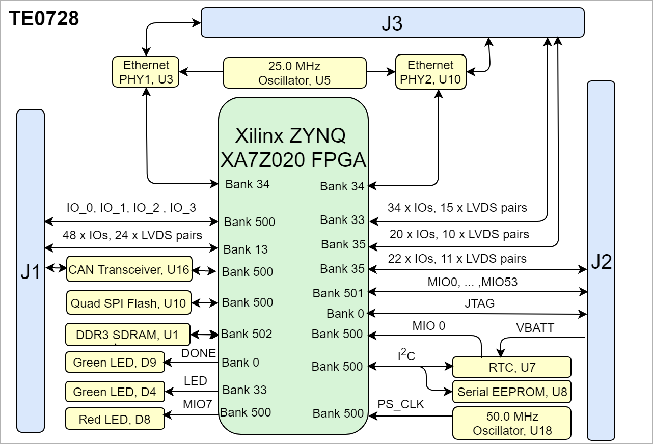 Image Added Image Added
|
|
Main Components
...
| Scroll Title |
|---|
| anchor | Table_OV_BP |
|---|
| title | Boot process. |
|---|
|
| Scroll Table Layout |
|---|
| orientation | portrait |
|---|
| sortDirection | ASC |
|---|
| repeatTableHeaders | default |
|---|
| style | |
|---|
| widths | |
|---|
| sortByColumn | 1 |
|---|
| sortEnabled | false |
|---|
| cellHighlighting | true |
|---|
|
MIO pin | Signal State | Boot Mode |
|---|
MIO4 | Low | QSPI | | MIO4 | High | SD Card |
|
Zynq-7020SoC includes a reset that is driven by the reset system. Hardware resets are driven by the power-on reset signal (PS_POR_B) and the system reset signal (PS_SRST_B).
| Scroll Title |
|---|
| anchor | Table_OV_RST |
|---|
| title | Reset process. |
|---|
|
| Scroll Table Layout |
|---|
| orientation | portrait |
|---|
| sortDirection | ASC |
|---|
| repeatTableHeaders | default |
|---|
| style | |
|---|
| widths | |
|---|
| sortByColumn | 1 |
|---|
| sortEnabled | false |
|---|
| cellHighlighting | true |
|---|
|
Signal | FPGA Bank | Pin | B2B |
|---|
PS_POR_B | 500 | B5 | JM2-9 | | PS_SRST_B | 501 | C9 | JM2-2 |
|
Signals, Interfaces and Pins
...
| Scroll Title |
|---|
| anchor | Table_SIP_B2B |
|---|
| title | General PL I/O to B2B connectors information |
|---|
|
| Scroll Table Layout |
|---|
| orientation | portrait |
|---|
| sortDirection | ASC |
|---|
| repeatTableHeaders | default |
|---|
| style | |
|---|
| widths | |
|---|
| sortByColumn | 1 |
|---|
| sortEnabled | false |
|---|
| cellHighlighting | true |
|---|
|
| FPGA Bank | B2B Connector | I/O Signal Count | Voltage Level | Notes |
|---|
| 13 | JM1 | 48 | VCCO_13 |
| | 500 | JM1 | 4 | 3.3V |
| | 33 | JM3 | 34 | 3.3V |
| | 35 | JM3 | 20 | 3.3V |
| | 35 | JM2 | 22 | 3.3V |
| | 501 | JM2 | 38 | VMIO1 | MIO1 VREF is connected to resistor divider to support HSTL18 |
|
JTAG Interface
JTAG access to the Xilinx XA7Z020 FPGA through B2B connector JM2.
| Scroll Title |
|---|
| anchor | Table_SIP_JTG |
|---|
| title | JTAG pins connection |
|---|
|
| Scroll Table Layout |
|---|
| orientation | portrait |
|---|
| sortDirection | ASC |
|---|
| repeatTableHeaders | default |
|---|
| style | |
|---|
| widths | |
|---|
| sortByColumn | 1 |
|---|
| sortEnabled | false |
|---|
| cellHighlighting | true |
|---|
|
JTAG Signal | B2B Pin |
|---|
| TMS | JM2-12 | | TDI | JM2-10 | | TDO | JM2-8 | | TCK | JM2-6 |
|
MIO Pins
| Scroll Title |
|---|
| anchor | Table_OBP_MIOs |
|---|
| title | MIOs pins |
|---|
|
| Scroll Table Layout |
|---|
| orientation | portrait |
|---|
| sortDirection | ASC |
|---|
| repeatTableHeaders | default |
|---|
| style | |
|---|
| widths | |
|---|
| sortByColumn | 1 |
|---|
| sortEnabled | false |
|---|
| cellHighlighting | true |
|---|
|
| MIO Pin | Schematic | Notes |
|---|
| MIO0 | MIO0 | RTC interrupt | | MIO1 | SPI_CS | SPI Flash | | MIO2 | SPI_DQ0/M0 | SPI Flash | | MIO3 | SPI_DQ1/M1 | SPI Flash | | MIO4 | SPI_DQ2/M2 | SPI Flash | | MIO5 | SPI_DQ3/M3 | SPI Flash | | MIO6 | SPI_SCK/M4 | SPI Flash clock | | MIO7 | LED RED | LED | | MIO8 | D | CAN Transceiver | | MIO9 | R | CAN Transceiver | | MIO10 | IO_0 | JM1-7 | | MIO11 | IO_1 | JM1-9 | | MIO12 | IO_2 | JM1-11 | | MIO13 | IO_3 | JM1-13 | | MIO14 | SCL | EEPROM | | MIO15 | SDA | EEPROM | | MIO16-MIO53 | PS_MIOxx | Bank 501 |
|
UART
There is no fixed mapping for PS7 UART, if needed it can be mapped to free pins from MIO1 Bank or via EMIO to PL pins.
...
| Scroll Title |
|---|
| anchor | Table_OBP |
|---|
| title | On board peripherals |
|---|
|
| Scroll Table Layout |
|---|
| orientation | portrait |
|---|
| sortDirection | ASC |
|---|
| repeatTableHeaders | default |
|---|
| style | |
|---|
| widths | |
|---|
| sortByColumn | 1 |
|---|
| sortEnabled | false |
|---|
| cellHighlighting | true |
|---|
|
| Chip/Interface | Product | Notes |
|---|
| SPI Flash | U13 | 16 MByte Flash | | EEPROM | U11 | 64 Kbit EEPROM | | RTC | U7 | Real Time Clock | | DDR3 SDRAM | U1 | Volatile Memory | | Ethernet | U3, U10 |
| | CAN Transceiver | U16 |
| | User LED | D4 | Green LED |
|
Quad SPI Flash Memory
On-board QSPI flash memory is used to store initial FPGA configuration. Datasheet is provided in Texas Instruments. Besides FPGA configuration, remaining free flash memory can be used for user application and data storage. All four SPI data lines are connected to the FPGA allowing x1, x2 or x4 data bus widths. Maximum data rate depends on the selected bus width and clock frequency used.
...
| Scroll Title |
|---|
| anchor | Table_OBP_SPI |
|---|
| title | Quad SPI interface MIOs and pins |
|---|
|
| Scroll Table Layout |
|---|
| orientation | portrait |
|---|
| sortDirection | ASC |
|---|
| repeatTableHeaders | default |
|---|
| style | |
|---|
| widths | |
|---|
| sortByColumn | 1 |
|---|
| sortEnabled | false |
|---|
| cellHighlighting | true |
|---|
|
| MIO Pin | Schematic | Pin | Notes |
|---|
| MIO1 | SPI_CS | U13-A1 |
| | MIO2 | SPI_DQ0/M0 | U13-A2 |
| | MIO3 | SPI_DQ1/M1 | U13-F6 |
| | MIO4 | SPI_DQ2/M2 | U13-E4 |
| | MIO5 | SPI_DQ3/M3 | U13-A3 |
| | MIO6 | SPI_SCK/M4 | U13-A4 |
|
|
RTC
The RTC has an I2C Bus (2-wire SerialInterface) and offers temperature compensated time. The STC-Smart Temperature Compensation is calibrated in the factory and leads to a very high time-accuracy.
...
| Scroll Title |
|---|
| anchor | Table_OBP_RTC |
|---|
| title | I2C interface MIOs and pins |
|---|
|
| Scroll Table Layout |
|---|
| orientation | portrait |
|---|
| sortDirection | ASC |
|---|
| repeatTableHeaders | default |
|---|
| style | |
|---|
| widths | |
|---|
| sortByColumn | 1 |
|---|
| sortEnabled | false |
|---|
| cellHighlighting | true |
|---|
|
| MIO Pin | Schematic | Pin | Notes |
|---|
| MIO15 | SDA | U7-5 | On-board RTC, and EEPROM | | MIO14 | SCL | U7-4 | On-board RTC, and EEPROM |
|
EEPROM
The Microchip Technology Inc. 24xx64 is a 64 Kbit Electrically Erasable PROM. The device is organized as a single block of 8K x 8-bit memory with a 2-wire serial interface. Lowvoltage design permits operation down to 1.7V, with standby and active currents of only 1 μA and 3 mA, respectively. It has been developed for advanced, lowpower applications such as personal communications or data acquisition. The 24xx64 also has a page write capability for up to 32 bytes of data. Functional address lines allow up to eight devices on the same bus, for up to 512 Kbits address space.
...
| Scroll Title |
|---|
| anchor | Table_OBP_EEP |
|---|
| title | I2C EEPROM interface MIOs and pins |
|---|
|
| Scroll Table Layout |
|---|
| orientation | portrait |
|---|
| sortDirection | ASC |
|---|
| repeatTableHeaders | default |
|---|
| style | |
|---|
| widths | |
|---|
| sortByColumn | 1 |
|---|
| sortEnabled | false |
|---|
| cellHighlighting | true |
|---|
|
| MIO Pin | Schematic | Pin | Notes |
|---|
| MIO15 | SDA | U11-3 | On-board RTC, and EEPROM | | MIO14 | SCL | U11-1 | On-board RTC, and EEPROM |
|
LEDs
| Scroll Title |
|---|
| anchor | Table_OBP_LED |
|---|
| title | On-board LEDs |
|---|
|
| Scroll Table Layout |
|---|
| orientation | portrait |
|---|
| sortDirection | ASC |
|---|
| repeatTableHeaders | default |
|---|
| style | |
|---|
| widths | |
|---|
| sortByColumn | 1 |
|---|
| sortEnabled | false |
|---|
| cellHighlighting | true |
|---|
|
| Schematic | Color | Connected to | Active Level | IO Standard |
|---|
| D9 | Green | DONE | Low | not applicable | | D8 | RED | MIO7 | High | not applicable | | D4 | Green | Bank 33 - V18 | High | LVCMOS33 |
|
DDR3 SDRAM
The TE0728 SoM has two 512 MByte volatile DDR3 SDRAM IC for storing user application code and data.
...
| Scroll Title |
|---|
| anchor | Table_OBP_ETH |
|---|
| title | Ethernet PHY to Zynq SoC connections |
|---|
|
| Scroll Table Layout |
|---|
| orientation | portrait |
|---|
| sortDirection | ASC |
|---|
| repeatTableHeaders | default |
|---|
| style | |
|---|
| widths | |
|---|
| sortByColumn | 1 |
|---|
| sortEnabled | false |
|---|
| cellHighlighting | true |
|---|
|
| Schematic | ETH1 | ETH2 | Pullup | Notes |
|---|
| CTREF | J3-57 | J3-25 |
| Magnetics center tap voltage | | TD+ | J3-58 | J3-28 | on-board |
| | TD- | J3-56 | J3-26 | on-board |
| | RD+ | J3-52 | J3-22 | on-board |
| | RD- | J3-50 | J3-20 | on-board |
| | LED1 | J3-55 | J3-23 | on-board |
| | LED2 | J3-53 | J3-21 | on-board |
| | LED3 | J3-51 | J3-19 | on-board |
| | POWERDOWN/INT | L21 | R20 | on-chip | It is recommended to configure FPGA I/O as input with Pullup or as output driving 1 if Interrupt not used. | | RESET_N | M15 | R16 | on-chip | It is recommended to configure FPGA I/O as input with Pullup or as output (active low PHY Reset). |
|
It is recommended to add IOB TRUE constraint for the MII Interface pins.
...
| Scroll Title |
|---|
| anchor | Table_OBP_CAN |
|---|
| title | CAN Tranciever interface MIOs |
|---|
|
| Scroll Table Layout |
|---|
| orientation | portrait |
|---|
| sortDirection | ASC |
|---|
| repeatTableHeaders | default |
|---|
| style | |
|---|
| widths | |
|---|
| sortByColumn | 1 |
|---|
| sortEnabled | false |
|---|
| cellHighlighting | true |
|---|
|
| MIO Pin | Schematic | Pin | Notes |
|---|
| MIO8 | D | U16-1 |
| | MIO9 | R | U16-4 |
|
|
Low Dropout Linear Regulator
...
| Scroll Title |
|---|
| anchor | Table_OBP_CLK |
|---|
| title | Osillators |
|---|
|
| Scroll Table Layout |
|---|
| orientation | portrait |
|---|
| sortDirection | ASC |
|---|
| repeatTableHeaders | default |
|---|
| style | |
|---|
| widths | |
|---|
| sortByColumn | 1 |
|---|
| sortEnabled | false |
|---|
| cellHighlighting | true |
|---|
|
| IC | Description | Frequency | Used as |
|---|
| U14 | MEMS Oscillator | 50 MHz | PS PLL clock | | U5 | MEMS Oscillator | 25 MHz | Ethernet PHY Clock | | U7 | RTC (internal oscillator) | 32.768 KHz | Used by RTC, CLKOUT of RTC not connected |
|
Power and Power-On Sequence
...
| Scroll Title |
|---|
| anchor | Table_PWR_PC |
|---|
| title | Power Consumption |
|---|
|
| Scroll Table Layout |
|---|
| orientation | portrait |
|---|
| sortDirection | ASC |
|---|
| repeatTableHeaders | default |
|---|
| style | |
|---|
| widths | |
|---|
| sortByColumn | 1 |
|---|
| sortEnabled | false |
|---|
| cellHighlighting | true |
|---|
|
| Power Input Pin | Typical Current |
|---|
| VIN | TBD* |
|
* TBD - To Be Determined
Power on Sequence
...
| Scroll Title |
|---|
| anchor | Figure_PWR_PS |
|---|
| title | Power Sequence |
|---|
|
| Scroll Ignore |
|---|
| draw.io Diagram |
|---|
| border | truefalse |
|---|
| viewerToolbar | true |
|---|
| |
|---|
| fitWindow | false |
|---|
| diagramDisplayName | |
|---|
| lbox | false |
|---|
| revision | 1 |
|---|
| diagramName | TE7028_PWR_PD |
|---|
| simpleViewer | false |
|---|
| width | 400 |
|---|
| links | auto |
|---|
| tbstyle | hidden |
|---|
| diagramWidth | 601 | revision | 1 |
|---|
|
|
|
...
| Scroll Title |
|---|
| anchor | Table_PWR_PR |
|---|
| title | Module power rails. |
|---|
|
| Scroll Table Layout |
|---|
| orientation | portrait |
|---|
| sortDirection | ASC |
|---|
| repeatTableHeaders | default |
|---|
| style | |
|---|
| widths | |
|---|
| sortByColumn | 1 |
|---|
| sortEnabled | false |
|---|
| cellHighlighting | true |
|---|
|
B2B Name | B2B JM1 Pin | B2B JM2 Pin | B2B JM3 Pin | Direction | Notes |
|---|
| VIN | 1,3 | - | - | Input | Supply voltage from carrier board. | | VCCO_13 | 39 | - | - | I/O |
| | VBATT | - | 1 | - | Output | RTC Supply voltage | | 3.3V | 19 | 2, 4 | 25,57 | Output | Internal 3.3V voltage level. | 1.8V | - | 5 | - | Output | Internal 1.8V voltage level. |
|
Bank Voltages
| Scroll Title |
|---|
| anchor | Table_PWR_BV |
|---|
| title | Zynq SoC bank voltages. |
|---|
|
| Scroll Table Layout |
|---|
| orientation | portrait |
|---|
| sortDirection | ASC |
|---|
| repeatTableHeaders | default |
|---|
| style | |
|---|
| widths | |
|---|
| sortByColumn | 1 |
|---|
| sortEnabled | false |
|---|
| cellHighlighting | true |
|---|
|
| Schematic Name | | Notes |
|---|
| 500 | VCCO_MIO0_500 | 3.3V |
| | 501 | VCCO_MIO1_500 | 3.3V |
| | 502 | VCCO_DDR_502 | 1.5V |
| | 13 HR | VCCO_13 | 3.3V | Supplied by the carrier board. JM1 | | 33 HR | VCCO_33 | 3.3V | Supplied by carrier board. JM3 | | 34 HR | VCCO_34 | 3.3V |
| | 35 HR | VCCO_35 | 3.3V | Supplied by the carrier board. JM2,JM3 |
|
Board to Board Connectors
...
| Scroll Title |
|---|
| anchor | Table_TS_AMR_PS |
|---|
| title | PS absolute maximum ratings |
|---|
|
| Scroll Table Layout |
|---|
| orientation | portrait |
|---|
| sortDirection | ASC |
|---|
| repeatTableHeaders | default |
|---|
| style | |
|---|
| widths | |
|---|
| sortByColumn | 1 |
|---|
| sortEnabled | false |
|---|
| cellHighlighting | true |
|---|
|
| Symbols | Description | Min | Max | Unit |
|---|
| VCCPINT | PS internal logic supply voltage | -0.5 | 1.1 | V | | VCCPAUX | PS auxiliary supply voltage | -0.5 | 2.0 | V | | VCCPLL | PS PLL supply | -0.5 | 2.0 | V | | VCCO_DDR | PS DDR I/O supply voltage | -0.5 | 2.0 | V | | VPREF | PS input reference voltage | -0.5 | 2.0 | V | | VCCO_MIO0 | PS MIO I/O supply voltage for HR I/O banks | -0.5 | 3.6 | V | | VCCO_MIO1 | PS MIO I/O supply voltage for HR I/O banks | 1.71 | 3.45 | V |
|
Programmable Logic(PL)
| Scroll Title |
|---|
| anchor | Table_TS_AMR_PL |
|---|
| title | PL absolute maximum ratings |
|---|
|
| Scroll Table Layout |
|---|
| orientation | portrait |
|---|
| sortDirection | ASC |
|---|
| repeatTableHeaders | default |
|---|
| style | |
|---|
| widths | |
|---|
| sortByColumn | 1 |
|---|
| sortEnabled | false |
|---|
| cellHighlighting | true |
|---|
|
| Symbols | Description | Min | Max | Unit |
|---|
| VCCINT | PL internal logic supply voltage | -0.5 | 1.1 | V | | VCCPAUX | PL auxiliary supply voltage | -0.5 | 2.0 | V | | VCCPLL | PL PLL supply | -0.5 | 1.1 | V | | VPREF | PL input reference voltage | -0.5 | 2.0 | V | | VCCO | PL supply voltage for HR I/O banks | -0.5 | 3.6 | V | | VIN | I/O input voltage for HR I/O banks | 1.71 | 3.45 | V |
|
Recommended Operating Conditions
...
| Scroll Title |
|---|
| anchor | Table_TS_ROC |
|---|
| title | Recommended operating conditions |
|---|
|
| Scroll Table Layout |
|---|
| orientation | portrait |
|---|
| sortDirection | ASC |
|---|
| repeatTableHeaders | default |
|---|
| style | |
|---|
| widths | |
|---|
| sortByColumn | 1 |
|---|
| sortEnabled | false |
|---|
| cellHighlighting | true |
|---|
|
| Parameter | Min | Max | Units | Reference Document |
|---|
| VIN supply voltage | 3.5 | 60 | V | TPS54260-Q1 datasheets. | | Supply voltage for PS MIO banks | 1.71 | 3.465 | V | See Xilinx DS187 datasheet. | | I/O input voltage for PS MIO banks | -0.2 | VCCO_MIO + 0.20 | V | See Xilinx DS187 datasheet. | | Supply voltage for PS DDR | 1.14 | 1.89 | V | See Xilinx DS187 datasheet. | | I/O input voltage for PS DDR | -0.20 | VCCO_DDR + 0.20 | V | See Xilinx DS187 datasheet. | | Supply voltage for HR I/Os banks | 1.14 | 3.465 | V | See Xilinx DS187 datasheet. | | I/O input voltage for HR I/O banks | -0.20 | VCCIO + 0.20 | V | See Xilinx DS187 datasheet. | | Storage Temperature | -65 | 150 | °C | See Xilinx DS187 datasheet. | | CAN Transceiver Temperature | -40 | 125 | °C | See Texas Instrument sn65hvd230q-q1 datasheet. | | SPI Flash Memory | -40 | 85 | °C | See Cypress S25FL127S datasheet. | | DDR3 SDRAM Temperature | -40 | 95 | °C | See Nanya NT5CC256M16CP-DIA datasheet. |
|
Temprature range: -40°C to +125°C.
...