...
| Scroll Title |
|---|
| anchor | Figure_OV_MC |
|---|
| title | TE0728 main components |
|---|
|
| Scroll Ignore |
|---|
| draw.io Diagram |
|---|
| border | false |
|---|
| viewerToolbar | true |
|---|
| |
|---|
| fitWindow | false |
|---|
| diagramDisplayName | |
|---|
| lbox | false |
|---|
| revision | 38 |
|---|
| diagramName | TE0728_MC2 |
|---|
| simpleViewer | true |
|---|
| width | 600 |
|---|
| links | auto |
|---|
| tbstyle | hidden |
|---|
| diagramWidth | 1173 |
|---|
|
|
| Scroll Only |
|---|
| scroll-pdf | true |
|---|
| scroll-office | true |
|---|
| scroll-chm | true |
|---|
| scroll-docbook | true |
|---|
| scroll-eclipsehelp | true |
|---|
| scroll-epub | true |
|---|
| scroll-html | true |
|---|
| | draw.io Diagram |
|---|
| border | false |
|---|
| viewerToolbar | true |
|---|
| fitWindow | false |
|---|
diagramDisplayName | | lbox | false |
|---|
| revision | 38 |
|---|
| diagramName | TE0728_MC2 |
|---|
| simpleViewer | true |
|---|
| width | 600 |
|---|
| links | auto |
|---|
| tbstyle | hidden |
|---|
| diagramWidth | 1173 |
|---|
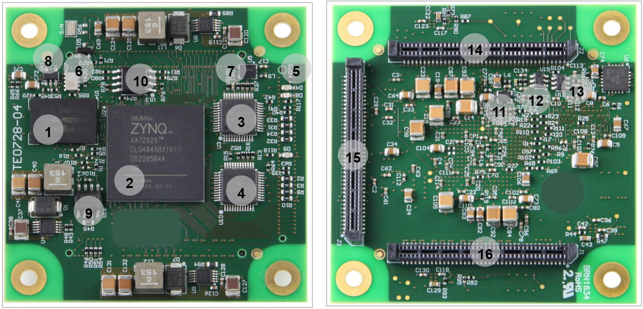 Image Added Image Added
|
|
- 512 MByte DDR3 SDRAM, Cypress DDR3 Memory, U1
- Xilinx Automotive XA7Z020-1CLG484Q ,U2
- 100 MBit Ethernet transceiver DP83848, U3
- 3.5V to 60V step-down converter, Texas Instruments TPS54260-Q1, U4
- Standard Clock Oscillators @ 25MHz 3.3V, SiTime SiT1618AA, U5
- 1.5 A Low Dropout Linear Regulator, Texas Instruments, TPS74801-Q1, U6
- Real Time Clock, Micro Crystal @32.768 MHz, 3.3V, RV-3029-C3, U7
- 3.5V to 60V step-down converter, Texas Instruments TPS54260-Q1, U8
- 3.5V to 60V step-down converter, Texas Instruments TPS54260-Q1, U9
- 100 MBit Ethernet transceiver DP83848MPHPEP, U10
- 64 Kbit I2C EEPROM, 24LC64, U11
- Low-Quiescent-Current Proggrammable Delay Supervisory Circuit, Texas Instruments TPS3808G01-Q1, U12
- 16 MByte QSPI Nor Flash memory, Cypress S25FL127, U13
- Standard Clock Oscillators @ 50MHz 3.3V, SiTime SiT8918AA, U14
- Low-Quiescent-Current Priggrammable Delay Supervisory Circuit, Texas Instruments TPS3808G01-Q1, U15
- CAN Tranceiver, Texas Instruments SN65HVD230Q1, U16
- B2B connector Samtec Micro Tiger Eye Connector SEM-140-02-03, JM2
- B2B connector Samtec Micro Tiger Eye Connector SEM-140-02-03, JM3
- B2B connector Samtec Micro Tiger Eye Connector SEM-140-02-03, JM1
- User LED Green
...
| Scroll Title |
|---|
| anchor | Figure_PWR_PS |
|---|
| title | Power On Sequence |
|---|
|
| Scroll Ignore |
|---|
| draw.io Diagram |
|---|
| border | false |
|---|
| viewerToolbar | true |
|---|
| |
|---|
| fitWindow | false |
|---|
| diagramDisplayName | |
|---|
| lbox | false |
|---|
| revision | 7 |
|---|
| diagramName | PWR_PS |
|---|
| simpleViewer | false |
|---|
| width | 600 |
|---|
| links | auto |
|---|
| tbstyle | hidden |
|---|
| diagramWidth | 641 |
|---|
|
|
| Scroll Only |
|---|
| scroll-pdf | true |
|---|
| scroll-office | true |
|---|
| scroll-chm | true |
|---|
| scroll-docbook | true |
|---|
| scroll-eclipsehelp | true |
|---|
| scroll-epub | true |
|---|
| scroll-html | true |
|---|
| 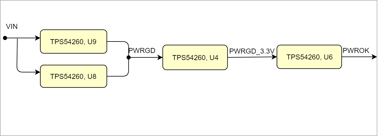 Image Added Image Added
|
|
Power Distribution Dependencies
| Scroll Title |
|---|
| anchor | Figure_PWR_PD |
|---|
| title | Power Dependencies |
|---|
|
| Scroll Ignore |
|---|
| draw.io Diagram |
|---|
| border | false |
|---|
| viewerToolbar | true |
|---|
| |
|---|
| fitWindow | false |
|---|
| diagramDisplayName | |
|---|
| lbox | false |
|---|
| revision | 1 |
|---|
| diagramName | TE7028_PWR_PD |
|---|
| simpleViewer | false |
|---|
| width | 400 |
|---|
| links | auto |
|---|
| tbstyle | hidden |
|---|
| diagramWidth | 601 |
|---|
|
|
| Scroll Only |
|---|
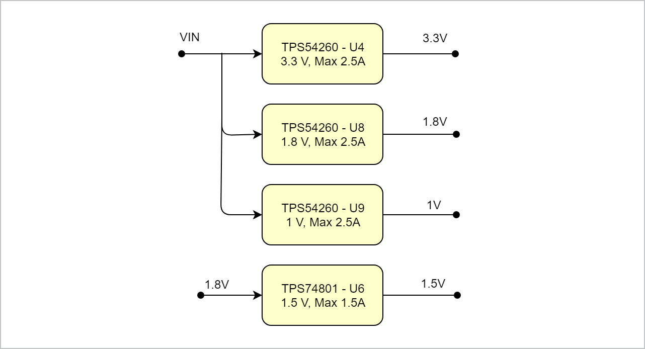 Image Added Image Added
|
|
The PS and PL power supplies are fully independent. PS power supplies (VCCPINT, VCCPAUX, VCCPLL, VCCO_DDR, VCCO_MIO0, and VCCO_MIO1) can be powered before or after any PL power supplies. The PS and PL power regions are isolated to prevent damage. The recommended power-on sequence is VCCPINT, then VCCPAUX and VCCPLL together, then the PS VCCO supplies (VCCO_MIO0, VCCO_MIO1, and VCCO_DDR) to achieve minimum current draw and ensure that the I/Os are 3-stated at power-on. The PS_POR_B input is required to be asserted to GND during the power-on sequence until VCCPINT, VCCPAUX and VCCO_MIO0 have reached minimum operating levels to ensure PS eFUSE integrity.
...