...
| Scroll Title |
|---|
| anchor | Figure_OV_MC |
|---|
| title | TE0728 main components |
|---|
|
| Scroll Ignore |
|---|
| draw.io Diagram |
|---|
| border | false |
|---|
| viewerToolbar | true |
|---|
| |
|---|
| fitWindow | false |
|---|
| diagramDisplayName | |
|---|
| lbox | false |
|---|
| revision | 39 |
|---|
| diagramName | TE0728_MC2 |
|---|
| simpleViewer | true |
|---|
| width | 600 |
|---|
| links | auto |
|---|
| tbstyle | hidden |
|---|
| diagramWidth | 1173 |
|---|
|
|
| Scroll Only |
|---|
| scroll-pdf | true |
|---|
| scroll-office | true |
|---|
| scroll-chm | true |
|---|
| scroll-docbook | true |
|---|
| scroll-eclipsehelp | true |
|---|
| scroll-epub | true |
|---|
| scroll-html | true |
|---|
| 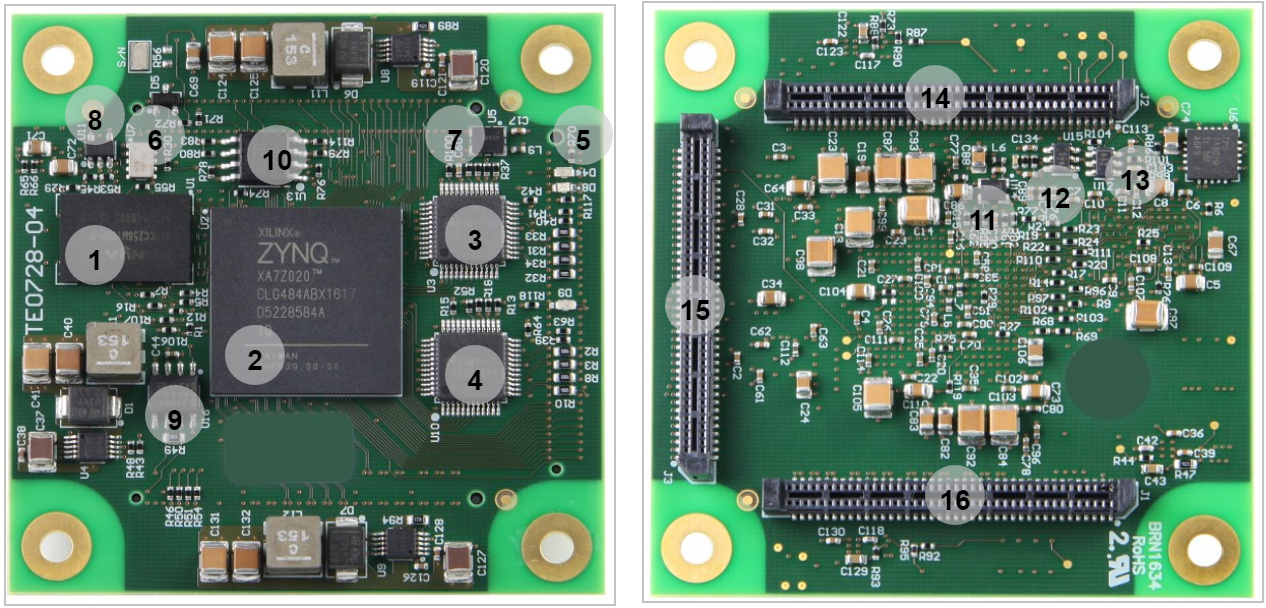 Image Modified Image Modified
|
|
- 512 MByte DDR3 SDRAM, U1
- Xilinx Automotive XA7Z020-1CLG484Q ,U2
- 100 MBit Ethernet transceiver, U3
- Standard Clock Oscillators @ 25MHz, U5
- 1.5 A Low Dropout Linear Regulator, U6
- Real Time Clock, Micro Crystal @32.768 MHz, U7
- 100 MBit Ethernet transceiver, U10
- 64 Kbit I2C EEPROM, U11
- Low-Quiescent-Current Proggrammable Delay Supervisory Circuit, U12
- 16 MByte QSPI Nor Flash memory, U13
- Standard Clock Oscillators @ 50MHz, U14
- Low-Quiescent-Current Priggrammable Delay Supervisory Circuit, U15
- CAN Tranceiver, U16
- B2B connector , JM2
- B2B connector , JM3
- B2B connector Samtec Micro Tiger Eye Connector SEM-140-02-03, JM1
- User LED Green
...
| Scroll Title |
|---|
| anchor | Table_OV_BP |
|---|
| title | Boot process. |
|---|
|
| Scroll Table Layout |
|---|
| orientation | portrait |
|---|
| sortDirection | ASC |
|---|
| repeatTableHeaders | default |
|---|
| style | |
|---|
| widths | |
|---|
| sortByColumn | 1 |
|---|
| sortEnabled | false |
|---|
| cellHighlighting | true |
|---|
|
Signal | FPGA Bank | Pin | B2B | Signal State | Boot Mode |
|---|
Boot_R | 500 | E4 | J2-11 | Low | QSPI | | High | SD Card |
|
Reset
Zynq-7020SoC includes a reset that is driven by the reset system. Hardware resets are driven by the power-on reset signal (Reset) connected to carrier and the system reset signal (PS_SRST_B) connected to VMIO, it means after power on the PS will be reset.
| Scroll Title |
|---|
| anchor | Table_OV_RST |
|---|
| title | Reset process. |
|---|
|
| Scroll Table Layout |
|---|
| orientation | portrait |
|---|
| sortDirection | ASC |
|---|
| repeatTableHeaders | default |
|---|
| style | |
|---|
| widths | |
|---|
| sortByColumn | 1 |
|---|
| sortEnabled | false |
|---|
| cellHighlighting | true |
|---|
|
Signal | B2B | I/O | Note |
|---|
Reset | J2-7 | Input | Comes from Carrier | | RST_OUT | J2-9 | OutOutput |
|
|
Signals, Interfaces and Pins
...
| Scroll Title |
|---|
| anchor | Table_OBP |
|---|
| title | On board peripherals |
|---|
|
| Scroll Table Layout |
|---|
| orientation | portrait |
|---|
| sortDirection | ASC |
|---|
| repeatTableHeaders | default |
|---|
| style | |
|---|
| widths | |
|---|
| sortByColumn | 1 |
|---|
| sortEnabled | false |
|---|
| cellHighlighting | true |
|---|
|
| Chip/Interface | Product | Notes |
|---|
| SPI Flash | U13 | 16 MByte Flash | | EEPROM | U11 | 64 Kbit EEPROM | | RTC | U7 | Real Time Clock | | DDR3 SDRAM | U1 | Volatile Memory | | Ethernet | U3, U10 |
| | CAN Transceiver | U16 |
| | User LED | D4 | Green LED |
|
Quad SPI Flash Memory
On-board QSPI flash memory is used to store initial FPGA configuration. Datasheet is provided in Texas Instruments. Besides FPGA configuration, remaining free flash memory can be used for user application and data storage. All four SPI data lines are connected to the FPGA allowing x1, x2 or x4 data bus widths. Maximum data rate depends on the selected bus width and clock frequency used.
Quad SPI Flash (U7) is connected to the Zynq PS QSPI0 interface via PS MIO bank 500.
...
| Scroll Title |
|---|
| anchor | Table_OBP_RTC |
|---|
| title | I2C interface MIOs and pins |
|---|
|
| Scroll Table Layout |
|---|
| orientation | portrait |
|---|
| sortDirection | ASC |
|---|
| repeatTableHeaders | default |
|---|
| style | |
|---|
| widths | |
|---|
| sortByColumn | 1 |
|---|
| sortEnabled | false |
|---|
| cellHighlighting | true |
|---|
|
| MIO Pin | Schematic | Pin | Notes |
|---|
| MIO15 | SDA | U7-5 | On-board RTC, and EEPROM | | MIO14 | SCL | U7-4 | On-board RTC, and EEPROM |
|
EEPROM
The Microchip Technology Inc. 24xx64 is a 64 Kbit Electrically Erasable PROM. The device is organized as a single block of 8K x 8-bit memory with a 2-wire serial interface. Lowvoltage design permits operation down to 1.7V, with standby and active currents of only 1 μA and 3 mA, respectively. It has been developed for advanced, lowpower applications such as personal communications or data acquisition. The 24xx64 also has a page write capability for up to 32 bytes of data. Functional address lines allow up to eight devices on the same bus, for up to 512 Kbits address space.
...
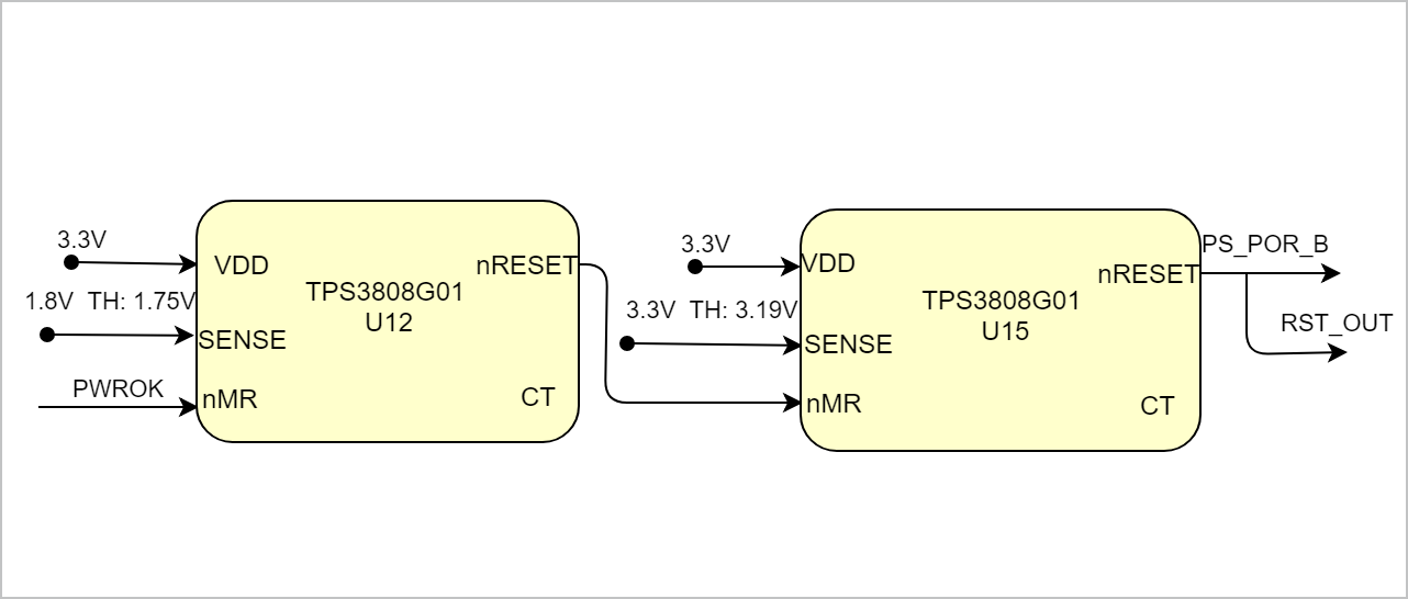
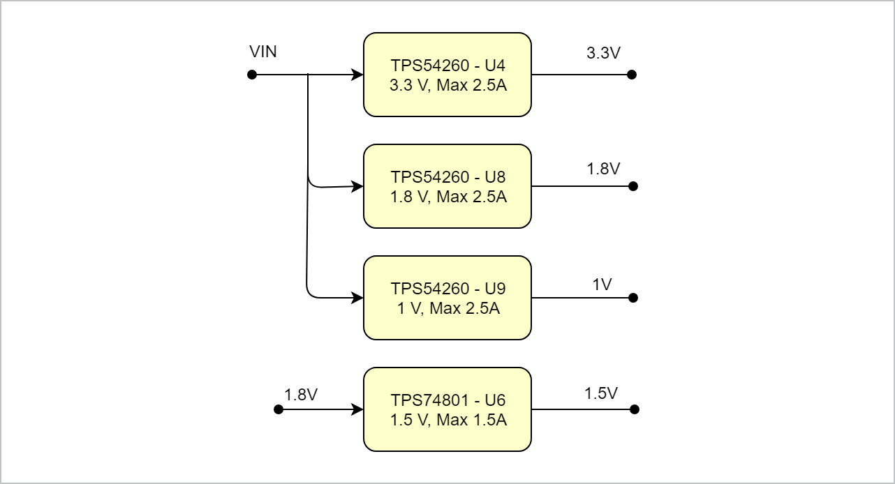
The PS and PL power supplies are fully independent. PS power supplies (VCCPINT, VCCPAUX, VCCPLL, VCCO_DDR, VCCO_MIO0, and VCCO_MIO1) can be powered before or after any PL power supplies. The PS and PL power regions are isolated to prevent damage. The recommended power-on sequence is VCCPINT, then VCCPAUX and VCCPLL together, then the PS VCCO supplies (VCCO_MIO0, VCCO_MIO1, and VCCO_DDR) to achieve minimum current draw and ensure that the I/Os are 3-stated at power-on. The PS_POR_B input is required to be asserted to GND during the power-on sequence until VCCPINT, VCCPAUX and VCCO_MIO0 have reached minimum operating levels to ensure PS eFUSE integrity.
| Scroll Title |
|---|
| anchor | Figure_PWR_PS |
|---|
| title | Power On Sequence |
|---|
|
| Scroll Ignore |
|---|
| scroll-pdf | true |
|---|
| scroll-office | true |
|---|
| scroll-chm | true |
|---|
| scroll-docbook | true |
|---|
| scroll-eclipsehelp | true |
|---|
| scroll-epub | true |
|---|
| scroll-html | true |
|---|
| | draw.io Diagram |
|---|
| border | false |
|---|
| viewerToolbar | true |
|---|
| |
|---|
| fitWindow | false |
|---|
| diagramDisplayName | |
|---|
| lbox | false |
|---|
| revision | 2 |
|---|
| diagramName | Figure_PWR_PS |
|---|
| simpleViewer | false |
|---|
| width | |
|---|
| links | auto |
|---|
| tbstyle | hidden |
|---|
| diagramWidth | 610 |
|---|
|
|
| Scroll Only |
|---|
| scroll-pdf | true |
|---|
| scroll-office | true |
|---|
| scroll-chm | true |
|---|
| scroll-docbook | true |
|---|
| scroll-eclipsehelp | true |
|---|
| scroll-epub | true |
|---|
| scroll-html | true |
|---|
| 
|
|
...
| Scroll Title |
|---|
| anchor | Figure_PWR_PD |
|---|
| title | Power Dependencies |
|---|
|
| Scroll Ignore |
|---|
| draw.io Diagram |
|---|
| border | false |
|---|
| viewerToolbar | true |
|---|
| |
|---|
| fitWindow | false |
|---|
| diagramDisplayName | |
|---|
| lbox | false |
|---|
| revision | 1 |
|---|
| diagramName | TE7028_PWR_PD |
|---|
| simpleViewer | false |
|---|
| width | |
|---|
| links | auto |
|---|
| tbstyle | hidden |
|---|
| diagramWidth | 601 |
|---|
|
|
| Scroll Only |
|---|
|
|
The PS and PL power supplies are fully independent. PS power supplies (VCCPINT, VCCPAUX, VCCPLL, VCCO_DDR, VCCO_MIO0, and VCCO_MIO1) can be powered before or after any PL power supplies. The PS and PL power regions are isolated to prevent damage. The recommended power-on sequence is VCCPINT, then VCCPAUX and VCCPLL together, then the PS VCCO supplies (VCCO_MIO0, VCCO_MIO1, and VCCO_DDR) to achieve minimum current draw and ensure that the I/Os are 3-stated at power-on. The PS_POR_B input is required to be asserted to GND during the power-on sequence until VCCPINT, VCCPAUX and VCCO_MIO0 have reached minimum operating levels to ensure PS eFUSE integrity.
Voltage Monitor Circuit
Voltage Monitor Circuit
The microprocessor supervisory circuits monitor system voltages asserting an open-drain RESET signal when the SENSE voltage drops The microprocessor supervisory circuits monitor system voltages from 0.4 V to 5 V, asserting an open-drain RESET signal when the SENSE voltage drops below a preset threshold or when the manual reset (MR) pin drops to a logic low. The RESET output remains low for the user adjustable delay time after the SENSE voltage and MR return above their thresholds. Datasheet is available in Texas Instruments website.
...
| Scroll Title |
|---|
| anchor | Table_PWR_PR |
|---|
| title | Module power rails. |
|---|
|
| Scroll Table Layout |
|---|
| orientation | portrait |
|---|
| sortDirection | ASC |
|---|
| repeatTableHeaders | default |
|---|
| style | |
|---|
| widths | |
|---|
| sortByColumn | 1 |
|---|
| sortEnabled | false |
|---|
| cellHighlighting | true |
|---|
|
B2B Name | B2B JM1 Pin | B2B JM2 Pin | B2B JM3 Pin | Direction | Notes |
|---|
| VIN | 1,3 | - | - | Input | Supply voltage from carrier board. | | VCCO_13 | 39 | - | - | I/O |
| | VBATT | - | 1 | - | Output | RTC Supply voltage | | 3.3V | 19 | 2, 4 | 25,57 | Output | Internal 3.3V voltage level. | 1.8V | - | 5 | - | Output | Internal 1.8V voltage level. |
|
...
| Scroll Title |
|---|
| anchor | Table_PWR_BV |
|---|
| title | Zynq SoC bank voltages. |
|---|
|
| Scroll Table Layout |
|---|
| orientation | portrait |
|---|
| sortDirection | ASC |
|---|
| repeatTableHeaders | default |
|---|
| style | |
|---|
| widths | |
|---|
| sortByColumn | 1 |
|---|
| sortEnabled | false |
|---|
| cellHighlighting | true |
|---|
|
| Schematic Name | | Notes |
|---|
| 500 | VCCO_MIO0_500 | 3.3V |
| | 501 | VCCO_MIO1_500 | Variable |
| | 502 | VCCO_DDR_502 | 1.5V |
| | 13 HR | VCCO_13 | Variable | Supplied by the carrier board. |
JM1| J1 | | 33 HR | 3.3V | 3.3V | Supplied by carrier board. |
JM3| J3 | | 34 HR | 3.3V | 3.3V |
| | 35 HR | 3.3V | 3.3V | Supplied by the carrier board. |
JM2JM3
|
Board to Board Connectors
...