...
| HTML |
|---|
<!-- tables have all same width (web max 1200px and pdfPDF full page(640px), flexible width or fix width on menu for single column can be used as before) -->
<style>
.wrapped{
  width: 100% !important;
  max-width: 1200px !important;
 }
</style> |
...
| Page properties |
|---|
|
Important General Note:
|
| Page properties |
|---|
|
----------------------------------------------------------------------- |
...
| Page properties |
|---|
|
Note for Download Link of the Scroll ignore macro: |
| Scroll pdf ignore |
|---|
Table of Contents |
Overview
Trenz Electronic TE0728 is an automotive-grade FPGA module integrating a Xilinx Automotive Zynq-7020 FPGA, two 100 Mbit Ethernet transceivers (PHY) , 512 MByte DDR3L SDRAM, 16 MByte Flash memory for configuration and operation, and powerful switching-mode power supplies for all on-board voltages. Numerous configurable I/Os are provided via rugged high-speed strips.
Within the complete module only Automotive components are installed.
All this in a compact 6 x 6 cm form factor, at the most competitive price.The Trenz Electronic TEB0728 Carrier Board provides functionalities for testing, evaluation and development purposes of company's 6 x 6 cm SoMs. The Carrier Board is equipped with various components and connectors for different configuration setups. See "6 x 6 SoM" Carriers" page for more information about 6 x 6 cm SoMs.
Refer to http://trenz.org/te0728TEB0728-info for the current online version of this manual and other available documentation.
Key Features
- Samtec Tiger Eye Terminal Socket ( 80 pins, 2 rows)
- Micro SD card socket
- 3 User LEDs, Red, Yellow, Green
- Two RJ45 Gigabit Ethernet socket
- Trenz 6x6 module connector strips (3 x Samtec Tiger Eye series connectors)
- Barrel Jack for 12V 5V power supply
- One user push button
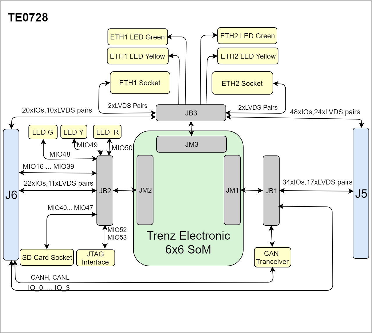
Block Diagram
| Scroll Title |
|---|
| anchor | Figure_OV_BD |
|---|
| title | TE0728 TEB0728 block diagram |
|---|
|
| Scroll Ignore |
|---|
true| false | | viewerToolbar | true |
|---|
| |
|---|
| fitWindow | false |
|---|
| diagramDisplayName | |
|---|
| lbox | true |
|---|
| revision |
|---|
|
3BD| BD1 | | simpleViewer | false |
|---|
| width | |
|---|
| links | auto |
|---|
| tbstyle | hidden |
|---|
| diagramWidth | 641 |
|---|
|
|
| Scroll Only |
|---|
 Image Removed Image Removed Image Added Image Added
|
|
Main Components
| Page properties |
|---|
|
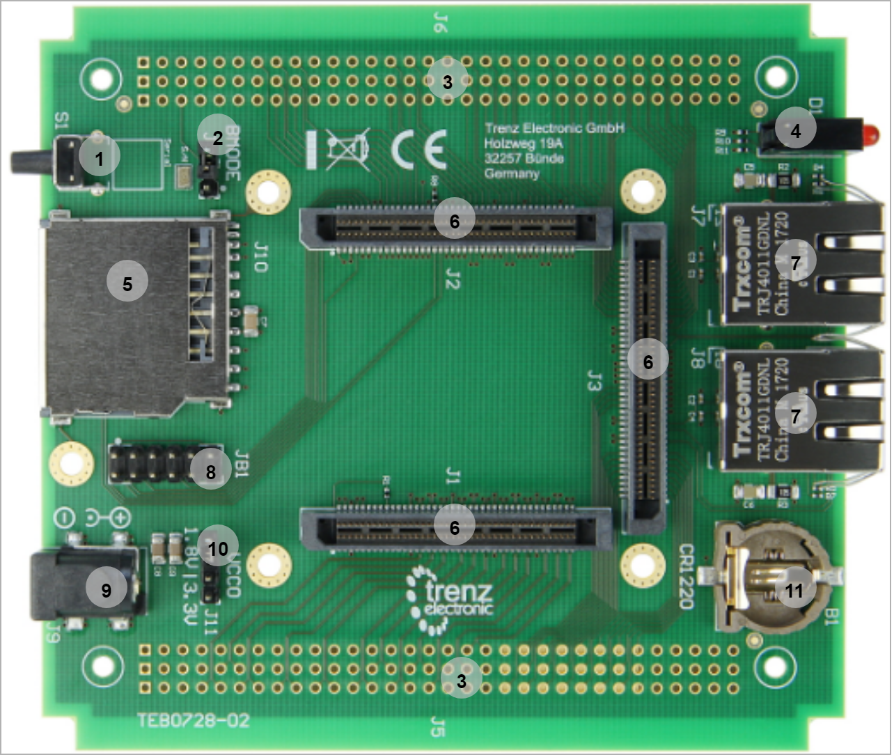
Notes : - Picture of the PCB (top and bottom side) with labels of important components
- Add List below
|
...
| Scroll Title |
|---|
| anchor | Figure_OV_MC |
|---|
| title | TE0728 TEB0728 main components |
|---|
|
| Scroll Ignore |
|---|
| draw.io Diagram |
|---|
| border | truefalse |
|---|
| viewerToolbar | true |
|---|
| |
|---|
| fitWindow | false |
|---|
| diagramDisplayName | |
|---|
| lbox | true |
|---|
| revision | 521 |
|---|
| diagramName | TE0728_MC |
|---|
| simpleViewer | false |
|---|
| width | |
|---|
| links | auto |
|---|
| tbstyle | hidden |
|---|
| diagramWidth | 641642 |
|---|
|
|
| Scroll Only |
|---|
 Image Modified Image Modified
|
|
- User push-button, S1
- Jumper (Boot Mode), J4
- External connector (VG96) placeholder, J5 / J6
- LEDs , D1
- Board to Board Connector, J1-J2-J3
- LEDs , D1
- CR1220 Backup-Battery holder, B1
- SD Card Connector, J10
- Board to Board Connector, J1-J2-J3
- RJ45 Gigabit Ethernet connector, J7-J8
- User push-button, S1
- Jumper, J4
- XMOD JTAG- / UART-header, JB1
- Barrel jack for 5V power supply, J9
- Jumper Jumper(VCCIO_13), J11External connector (VG96) placeholder, J5 / J6
- CR1220 Backup-Battery holder, B1
Initial Delivery State
There is no hardware component to be programmed on teh the carrier.
| Scroll Title |
|---|
| anchor | Table_OV_IDS |
|---|
| title | Initial delivery state of programmable devices on the module |
|---|
|
| Scroll Table Layout |
|---|
| orientation | portrait |
|---|
| sortDirection | ASC |
|---|
| repeatTableHeaders | default |
|---|
| style | |
|---|
| widths | |
|---|
| sortByColumn | 1 |
|---|
| sortEnabled | false |
|---|
| cellHighlighting | true |
|---|
|
Storage device name | Content | Notes |
|---|
|
Control Signals
Configuration Signals
| Page properties |
|---|
|
- Overview of Boot Mode, Reset, Enables,
|
Boot Process
| Scroll Title |
|---|
| anchor | Table_OV_BP |
|---|
| title | Boot process. |
|---|
|
| Scroll Table Layout |
|---|
| orientation | portrait |
|---|
| sortDirection | ASC |
|---|
| repeatTableHeaders | default |
|---|
| style | |
|---|
| widths | |
|---|
| sortByColumn | 1 |
|---|
| sortEnabled | false |
|---|
| cellHighlighting | true |
|---|
|
Signal | Designator | B2B | Signal LevelJumper | Boot Mode |
|---|
Boot_R | J4 | J2-11 | Open | QSPI | | Short | SD Card |
|
Reset Process
There is a user push button which is used for RESET signal.
| Scroll Title |
|---|
| anchor | Table_OV_BP |
|---|
| title | Reset process. |
|---|
|
| Scroll Table Layout |
|---|
| orientation | portrait |
|---|
| sortDirection | ASC |
|---|
| repeatTableHeaders | default |
|---|
| style | |
|---|
| widths | |
|---|
| sortByColumn | 1 |
|---|
| sortEnabled | false |
|---|
| cellHighlighting | true |
|---|
|
Signal | Designator | B2B | Active Level |
|---|
RESET | S1 | J2-7 | Active High |
|
Signals, Interfaces and Pins
| Page properties |
|---|
|
Notes : - For carrier or stand-alone boards use subsection for every connector type (add designator on description, not on the subsection title), for example:
- For modules which needs carrier use only classes and refer to B2B connector if more than one is used, for example
|
Board to Board (B2B) I/Os
FPGA bank number and number Number of I/O signals FPGA bank numbers connected to the B2B connectorconnectors:
| Scroll Title |
|---|
| anchor | Table_SIP_B2B |
|---|
| title | General overview of PL I/O signals and SoM's interfaces connected to the B2B connectors information. |
|---|
|
| Scroll Table Layout |
|---|
| orientation | portrait |
|---|
| sortDirection | ASC |
|---|
| repeatTableHeaders | default |
|---|
| style | |
|---|
| widths | |
|---|
| sortByColumn | 1 |
|---|
| sortEnabled | false |
|---|
| cellHighlighting | true |
|---|
|
| B2B Connector | Interfaces | Number of I/O | Notes |
|---|
J1
| User I/O | 48 singel ended, 24 differential | Connected to Bank 13 | | 4 Single ended | MIO10 |
-| ...13 | | CANH , CANL | 2 single ended | MIO8, MIO9 | J2
| User I/O | 22 singel ended, 11 differential |
| | 38 single ended | MIO16 |
-| ...53 | | SoM Control Signals | 5 | RESET, RST_OUT, BOOT_R, | | JTAG Interface | 4 | TCK , TDO, TDI, TMS | J3
| User I/O | 20 Single ended, 10 differential
| Connected to Bank 35 | | 34 single ended, 17 differential | Connected to Bankd 33 |
|
JTAG Interface
JTAG access to the Xilinx XXXXXXX FPGA through B2B connector JM2.
...
| anchor | Table_SIP_JTG |
|---|
| title | JTAG pins connection |
|---|
...
JTAG Signal
...
B2B Pin
...
| Page properties |
|---|
|
Notes : - add subsection for every component which is important for design, for example:
- Two 100 Mbit Ethernet Transciever PHY
- USB PHY
- Programmable Clock Generator
- Oscillators
- eMMCs
- RTC
- FTDI
- ...
- DIP-Switches
- Buttons
- LEDs
|
...
| anchor | Table_OBP |
|---|
| title | On board peripherals |
|---|
...
| Ethernet 1 | 4 single ended, 2 differential | ETH_CTREF , ETH_TD+, ETH_TD- , ETH_RD+, ETH_RD-, ETH_LED1, ETH_LED2, ETH_LED3 | | Ethernet 2 | 4 single ended, 2 differential | ETH_CTREF , ETH_TD+, ETH_TD- , ETH_RD+, ETH_RD-, ETH_LED1, ETH_LED2, ETH_LED3 |
|
On-board Connector
There are two pin placeholder on the board, J5-J6.
| Scroll Title |
|---|
| anchor | Table_SIP_OnB |
|---|
| title | General information about On-board connectors information |
|---|
|
| Scroll Table Layout |
|---|
| orientation | portrait |
|---|
| sortDirection | ASC |
|---|
| repeatTableHeaders | default |
|---|
| style | |
|---|
| widths | |
|---|
| sortByColumn | 1 |
|---|
| sortEnabled | false |
|---|
| cellHighlighting | true |
|---|
|
| VGA96 Vertical Connector | Interfaces | Number of I/O | Notes |
|---|
J5
| User I/O | 48 singel ended, 24 differential | Connected to Bank 13 | | 34 single ended, 17 differential | Connected to Bank 33 | J6
| User I/O | 42 singel ended, 21 differential |
| | 27 single ended | MIO16... MIO39 + MIO51...53 | | 4 single ended | MIO10...13 | | SoM Control Signals | 3 | RESET, RST_OUT, BOOT_R | | JTAG Interface | 4 | TCK , TDO, TDI, TMS | CANH , CANL | 2 single ended | MIO8, MIO9 |
|
JTAG Interface Base
JTAG access to the TEB0728 Trenz module is available through B2B connector J2. JTAG Programmer TE0790_02 is provided by Trenz Electronic, More information is available here.
| Scroll Title |
|---|
| anchor | Table_SIP_JTG |
|---|
| title | JTAG interface Base |
|---|
|
On-board QSPI flash memory S25FL127SABMFV10 is used to store initial FPGA configuration. Datasheet is provided in Texas Instruments. Besides FPGA configuration, remaining free flash memory can be used for user application and data storage. All four SPI data lines are connected to the FPGA allowing x1, x2 or x4 data bus widths. Maximum data rate depends on the selected bus width and clock frequency used.
Quad SPI Flash (U7) is connected to the Zynq PS QSPI0 interface via PS MIO bank 500.
| Scroll Title |
|---|
| anchor | Table_OBP_SPI |
|---|
| title | Quad SPI interface MIOs and pins |
|---|
|
| Scroll Table Layout |
|---|
| orientation | portrait |
|---|
| sortDirection | ASC |
|---|
| repeatTableHeaders | default |
|---|
| style | |
|---|
| widths | |
|---|
| sortByColumn | 1 |
|---|
| sortEnabled | false |
|---|
| cellHighlighting | true |
|---|
|
MIO | Schematic | U13 Pin | Notes | |
...
| anchor | Table_OBP_RTC |
|---|
| title | I2C interface MIOs and pins |
|---|
...
EEPROM
...
| anchor | Table_OBP_EEP |
|---|
| title | I2C EEPROM interface MIOs and pins |
|---|
| XMOD Header JB1 | Note |
|---|
| A | J2-15 | JB1-3 | UART Txd - input | | B | J2-16 | JB1-7 | UART Rxd - Output | | C | J2-12 | JB1-4 | JTAG-TMS | | D | J2-10 | JB1-8 | JTAG-TDI | | F | J2-8 | JB1-10 | JTAG-TDO | | H | J2-6 | JB1-12 | JTAG-TCK | | G | J2-7 | JB1-11 | RESET will be connected to Push Button on JTAG Programmer | | 3.3V | - | JB1-5 | connected to GND | | VIO | J2-2/4 | JB1-6 | VIO is connected to 3.3V which is supplied by carrier |
|
SD Card Socket
Power supply voltage for SD card holder is 3.3V.
...
| Scroll Title |
|---|
| anchor | Table_OBP_LED |
|---|
| title | On - board LEDsperipherals |
|---|
|
| Scroll Table Layout |
|---|
| orientation | portrait |
|---|
| sortDirection | ASC |
|---|
| repeatTableHeaders | default |
|---|
| style | |
|---|
| widths | |
|---|
| sortByColumn | 1 |
|---|
| sortEnabled | false |
|---|
| cellHighlighting | true |
|---|
|
| Signals | B2B | NotesSchematic | Color | Connected to | Active Level | IO Standard |
|---|
|
...
| CMD | J2-29 |
| | CLK | J2-34 |
| | DAT0 | J2-37 |
| | DAT1 | J2-40 |
| | DAT2 | J2-32 |
| | CD/DAT3 | J2-31 |
| | CD | J2-35 |
| | WP | J2-33 |
|
|
RJ45 Connector
Both Ethernet sockets,ETH1 and ETH2, are connected to the Board to Board (B2B) J3 on the carrier.
| Scroll Title |
|---|
| anchor | Table_OBP_ETH |
|---|
| title | Ethernet Connections to B2B Connectors |
|---|
|
|
...
The TE0728 SoM has XXX GByte volatile DDR3 SDRAM IC for storing user application code and data.
- Part number:
- Supply voltage:
- Speed:
- NOR Flash
- Temperature:
Ethernet
| Scroll Title |
|---|
| anchor | Table_OBP_ETH |
|---|
| title | Ethernet PHY to Zynq SoC connections |
|---|
|
| Scroll Table Layout |
|---|
| orientation | portrait |
|---|
| sortDirection | ASC |
|---|
| repeatTableHeaders | default |
|---|
| style | |
|---|
| widths | |
|---|
| sortByColumn | 1 |
|---|
| sortEnabled | false |
|---|
| cellHighlighting | true |
|---|
|
SchematicPullup| CTREF | TDRDRD+ | LED1 | LED2 | LED3 | POWERDOWN/INT | RESET_N | |
CAN Transceiver
...
| anchor | Table_OBP_CAN |
|---|
| title | CAN Tranciever interface MIOs |
|---|
| Transfer | | ETH_TD- | J3-56 | J3-26 |
| | ETH_RD+ | J3_52 | J3-22 | Receive | | ETH_RD- | J3-50 | J3-20 |
| | ETH_CTREF | J3_57 | J3-25 |
| | ETH_LED1 | J3-55 | J3-23 | Yellow LED- Activity | | ETH_LED3 | J3-51 | J3-19 | Green Green- Link |
|
On-board Peripherals
| Page properties |
|---|
|
Notes : - add subsection for every component which is important for design, for example:
- Two 100 Mbit Ethernet Transciever PHY
- USB PHY
- Programmable Clock Generator
- Oscillators
- eMMCs
- RTC
- FTDI
- ...
- DIP-Switches
- Buttons
- LEDs
|
Push button
...
Low Quiescent Current Programmable Delay Supervisory Circuit
Low Dropout Linear Regulator
...
| Scroll Title |
|---|
| anchor | Table_OBP_Push_CLKButton |
|---|
| title | OsillatorsOn-board push button |
|---|
|
| Scroll Table Layout |
|---|
| orientation | portrait |
|---|
| sortDirection | ASC |
|---|
| repeatTableHeaders | default |
|---|
| style | |
|---|
| widths | |
|---|
| sortByColumn | 1 |
|---|
| sortEnabled | false |
|---|
| cellHighlighting | true |
|---|
|
| ICDesignator | DescriptionConnected to | Frequency | Used as | MEMS Oscillator | MHz | MEMS Oscillator | MHz | RTC (internal oscillator) | KHz |
|---|
|
...
Power Supply
Power supply with minimum current capability of 3.5 A for system startup is recommended.
Power Consumption
...
| anchor | Table_PWR_PC |
|---|
| title | Power Consumption |
|---|
...
Power Distribution Dependencies
...
| anchor | Figure_PWR_PD |
|---|
| title | Power Distribution |
|---|
| Scroll Ignore |
|---|
add drawIO object here: Attention if you copy from other page, objects are only linked. |
| Scroll Only |
|---|
image link to the generate drawIO PNG file of this page. This is a workaround until scroll pdf export bug is fixed |
| B2B | Active Level | Note |
|---|
| S1-A | RESET | J2-7 | Active high | General Input RESET |
|
Jumpers
Power-On Sequence
...
| anchor | Figure_PWR_PS |
|---|
| title | Power Sequency |
|---|
| Scroll Ignore |
|---|
Create DrawIO object here: Attention if you copy from other page, objects are only linked. |
| Scroll Only |
|---|
image link to the generate DrawIO PNG file of this page. This is a workaround until scroll pdf export bug is fixed |
...
| anchor | Table_PWR_PR |
|---|
| title | Module power rails. |
|---|
...
B2B Connector
JM1 Pin
...
B2B Connector
JM2 Pin
...
B2B Connector
JM3 Pin
...
Bank Voltages
...
| anchor | Table_PWR_BV |
|---|
| title | Zynq SoC bank voltages. |
|---|
...
...
...
...
6 x 6 modules use two or three Samtec Micro Tiger Eye Connector on the bottom side.
3 x REF-189018-01 (compatible to SEM-140-02-03.0-H-D-A), (80 pins, "40" per row)
Operating Temperature:-55°C ~ 125°C
Current Rating: 2.6A per ContactNumber of Positions: 80
Number of Rows: 2
Absolute Maximum Ratings
...
| Scroll Title |
|---|
| anchor | Table_TSOBP_AMR_PSJumpers |
|---|
| title | PS absolute maximum ratingsOn-board Jumpers |
|---|
|
| Scroll Table Layout |
|---|
| orientation | portrait |
|---|
| sortDirection | ASC |
|---|
| repeatTableHeaders | default |
|---|
| style | |
|---|
| widths | |
|---|
| sortByColumn | 1 |
|---|
| sortEnabled | false |
|---|
| cellHighlighting | true |
|---|
|
|
| Symbols | Description | Min | Max | Unit |
|---|
| VCCPINT | PS internal logic supply voltage | -0.5 | 1.1 | V |
| VCCPAUX | PS auxiliary supply voltage | -0.5 | 2.0 | V |
| VCCPLL | PS PLL supply | -0.5 | 2.0 | V |
| VCCO_DDR | PS DDR I/O supply voltage | -0.5 | 2.0 | V |
| VPREF | PS input reference voltage | -0.5 | 2.0 | V |
| VCCO_MIO0 | PS MIO I/O supply voltage for HR I/O banks | -0.5 | 3.6 | V |
| VCCO_MIO1 | PS MIO I/O supply voltage for HR I/O banks | 1.71 | 3.45 | V |
...
| Designator | Connected to | B2B | Note |
|---|
| J4 | Boot_R | J2-11 | Open: QSPI | | Short: SD Card |
|
| Scroll Title |
|---|
| anchor | Table_OBP_Jumpers |
|---|
| title | On-board Jumpers |
|---|
|
| Scroll Table Layout |
|---|
| orientation | portrait |
|---|
| sortDirection | ASC |
|---|
| repeatTableHeaders | default |
|---|
| style | |
|---|
| widths | |
|---|
| sortByColumn | 1 |
|---|
| sortEnabled | false |
|---|
| cellHighlighting | true |
|---|
|
| Designator | Connected to | Voltage | Note |
|---|
| J11 | VCCIO_13 | 3.3 V | Pin 1 and the middle pin are connected | | 1.8 V | Pin 3 and the middle pin are connected |
|
LEDs
...
| Scroll Title |
|---|
| anchor | Table_TSOBP_AMR_PLLED |
|---|
| title | PL absolute maximum ratingsOn-board LEDs |
|---|
|
| Scroll Table Layout |
|---|
| orientation | portrait |
|---|
| sortDirection | ASC |
|---|
| repeatTableHeaders | default |
|---|
| style | |
|---|
| widths | |
|---|
| sortByColumn | 1 |
|---|
| sortEnabled | false |
|---|
| cellHighlighting | true |
|---|
|
|
| Symbols | Description | Min | Max | Unit |
|---|
| VCCINT | PL internal logic supply voltage | -0.5 | 1.1 | V |
| VCCPAUX | PL auxiliary supply voltage | -0.5 | 2.0 | V |
| VCCPLL | PL PLL supply | -0.5 | 1.1 | V |
| VPREF | PL input reference voltage | -0.5 | 2.0 | V |
| VCCO | PL supply voltage for HR I/O banks | -0.5 | 3.6 | V |
| VIN | I/O input voltage for HR I/O banks | 1.71 | 3.45 | V |
Technical Specifications
Absolute Maximum Ratings
| Designator | Color | B2B | Active Level | Note |
|---|
| D1-A | Red | J2-30 | Active high |
| | D1-B | Yellow | J2-38 | Active high |
| | D1-C | Green | J2-36 | Active high |
|
|
Power and Power-On Sequence
Power Supply
| Note |
|---|
| No power supply protection circuit on the carrier, module will be powered directly |
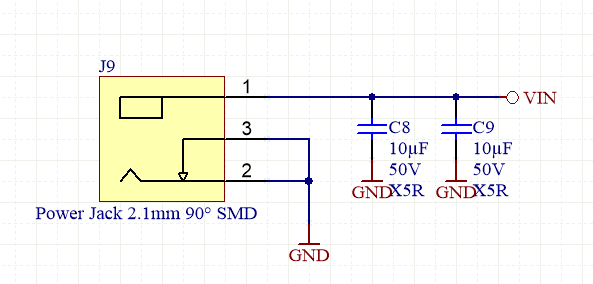
Single 5V power supply with minimum current capability of 2.5A is recommended to operate the board.
- 5V VIN (inner)
GND (outer)
| Scroll Title |
|---|
| anchor | Figure_pwr_connector |
|---|
| title | Power Connector |
|---|
|
 Image Added Image Added
|
Power Consumption
| Scroll Title |
|---|
| anchor | Table_PWR_PC |
|---|
| title | Power Consumption |
|---|
|
| Scroll Table Layout |
|---|
| orientation | portrait |
|---|
| sortDirection | ASC |
|---|
| repeatTableHeaders | default |
|---|
| style | |
|---|
| widths | |
|---|
| sortByColumn | 1 |
|---|
| sortEnabled | false |
|---|
| cellHighlighting | true |
|---|
|
| Power Input Pin | Typical Current |
|---|
| VIN | TBD* | | VBATT | TBD* |
|
* TBD - To Be Determined
Power Rails
| Scroll Title |
|---|
| anchor | Table_TSPWR_AMRPR |
|---|
| title | Module absolute maximum ratingsCarrier Power Rails. |
|---|
|
| Scroll Table Layout |
|---|
| orientation | portrait |
|---|
| sortDirection | ASC |
|---|
| repeatTableHeaders | default |
|---|
| style | |
|---|
| widths | |
|---|
| sortByColumn | 1 |
|---|
| sortEnabled | false |
|---|
| cellHighlighting | true |
|---|
|
|
| Parameter | Min | Max | Units | Reference Document |
|---|
| VIN supply voltage | 3.5 | 60 | V | TPS54260-Q1 datasheets. |
| Supply voltage for PS MIO banks | 1.71 | 3.465 | V | See Xilinx DS187 datasheet. |
| I/O input voltage for PS MIO banks | -0.2 | VCCO_MIO + 0.20 | V | See Xilinx DS187 datasheet. |
| Supply voltage for PS DDR | 1.14 | 1.89 | V | See Xilinx DS187 datasheet. |
| I/O input voltage for PS DDR | -0.20 | VCCO_DDR + 0.20 | V | See Xilinx DS187 datasheet. |
| Supply voltage for HR I/Os banks | 1.14 | 3.465 | V | See Xilinx DS187 datasheet. |
| I/O input voltage for HR I/O banks | -0.20 | VCCIO + 0.20 | V | See Xilinx DS187 datasheet. |
| Storage Temperature | -40 | 125 | °C | See Xilinx DS187 datasheet. |
...
Commercial grade: 0°C to +70°C.
Industrial and automotive grade: -40°C to +85°C.
...
| Module Connector (B2B) Designator | VCC / VCCIO | Direction | Pins | Notes |
|---|
| JB1 | VIN | Output | 1, 3 | Up to 12V carrier supply voltage | | 3.3V | Input | 19 | PL IO-bank VCCIO | | VCCO_13 | Output | 39 | 1.8V or 3.3V over jumper | | JB2 | 3.3V | Input | 2, 4 | 3.3V module supply voltage | | 1.8V | Input | 5 | PL IO-bank VCCIO | | VBATT | Output | 1 | RTC buffer voltage | | JB3 | - | - | - | - |
|
Board to Board Connectors
| Include Page |
|---|
| 6 x 6 SoM TEM and SEM B2B Connectors |
|---|
| 6 x 6 SoM TEM and SEM B2B Connectors |
|---|
|
Absolute Maximum Ratings
| Scroll Title |
|---|
| anchor | Table_TS_ROCAMR |
|---|
| title | Recommended operating conditionsModule absolute maximum ratings. |
|---|
|
| Scroll Table Layout |
|---|
| orientation | portrait |
|---|
| sortDirection | ASC |
|---|
| repeatTableHeaders | default |
|---|
| style | |
|---|
| widths | |
|---|
| sortByColumn | 1 |
|---|
| sortEnabled | false |
|---|
| cellHighlighting | true |
|---|
|
|
| Parameter | Min | Max | Units | Reference Document |
|---|
| VIN supply voltage | 3.5 | 60 | V | TPS54260-Q1 datasheets. |
| Supply voltage for PS MIO banks | 1.71 | 3.465 | V | See Xilinx DS187 datasheet. |
| I/O input voltage for PS MIO banks | -0.2 | VCCO_MIO + 0.20 | V | See Xilinx DS187 datasheet. |
| Supply voltage for PS DDR | 1.14 | 1.89 | V | See Xilinx DS187 datasheet. |
| I/O input voltage for PS DDR | -0.20 | VCCO_DDR + 0.20 | V | See Xilinx DS187 datasheet. |
| Supply voltage for HR I/Os banks | 1.14 | 3.465 | V | See Xilinx DS187 datasheet. |
| I/O input voltage for HR I/O banks | -0.20 | VCCIO + 0.20 | V | See Xilinx DS187 datasheet. |
| Storage Temperature | -65 | 150 | °C | See Xilinx DS187 datasheet. |
| CAN Transceiver Temperature | -40 | 125 | °C | See Texas Instrument sn65hvd230q-q1 datasheet. |
| SPI Flash Memory | -40 | 85 | °C | See Cypress S25FL127S datasheet. |
| DDR3 SDRAM Temperature | -40 | 95 | °C | See Nanya NT5CC256M16CP-DIA datasheet. |
...
| anchor | Figure_TS_PD |
|---|
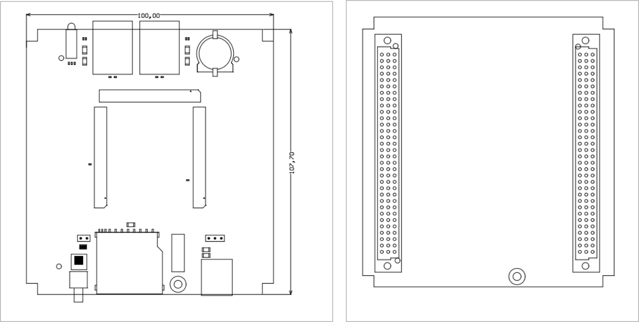
| title | Physical dimensions drawing |
|---|
| Parameter | Min | Max | Units | Note |
|---|
| VIN supply voltage | -- | -- | V | - Connected directly to the module power supply, see Module TRM
| | Storage Temperature | -25 | +85 | °C |
|
|
Recommended Operating Conditions
Operating temperature range depends also on customer design and cooling solution. Please contact us for options.
| Scroll Title |
|---|
| anchor | Table_TS_ROC |
|---|
| title | Recommended operating conditions. |
|---|
|
| Scroll Table Layout |
|---|
| orientation | portrait |
|---|
| sortDirection | ASC |
|---|
| repeatTableHeaders | default |
|---|
| style | |
|---|
| widths | |
|---|
| sortByColumn | 1 |
|---|
| sortEnabled | false |
|---|
| cellHighlighting | true |
|---|
|
| Parameter | Min | Max | Units | Note |
|---|
| VIN supply voltage | -- | -- | V | - Connected directly to the module power supply, see Module TRM
- 5V recommended for usage with TE0728
| | Operating Temperature | -25 | +85 | °C |
|
|
Physical Dimensions
Module size: 100 mm × 107.7 Module size: 60 mm × 60 mm. Please download the assembly diagram for exact numbers.
Mating height with standard connectors: 7 mm.
PCB thickness: 1.6 mm.
| Scroll Title |
|---|
| anchor | Figure_TS_PD |
|---|
| title | Physical Dimension |
|---|
|
| Scroll Ignore |
|---|
| draw.io Diagram |
|---|
| border | true |
|---|
| viewerToolbar | true |
|---|
| |
|---|
| fitWindow | false |
|---|
| diagramDisplayName | |
|---|
| lbox | true |
|---|
| revision | 8 |
|---|
| diagramName | Figure_TS_PD |
|---|
| simpleViewer | false |
|---|
| width | |
|---|
| links | auto |
|---|
| tbstyle | hidden |
|---|
| diagramWidth | 656 |
|---|
|
|
|
| anchor | Figure_TS_PD |
|---|
title | Physical Dimension
| Scroll Only |
|---|
| scroll-pdf | true |
|---|
| scroll-office | true |
|---|
| scroll-chm | true |
|---|
| scroll-docbook | true |
|---|
| scroll-eclipsehelp | true |
|---|
| scroll-epub | true |
|---|
| scroll-html | true |
|---|
|
|
...
 Image Added Image Added
|
|
Currently Offered Variants
...
| Scroll Title |
|---|
| anchor | Table_VCP_SO |
|---|
| title | Trenz Electronic Shop Overview |
|---|
|
| Scroll Table Layout |
|---|
| orientation | portrait |
|---|
| sortDirection | ASC |
|---|
| repeatTableHeaders | default |
|---|
| style | |
|---|
| widths | |
|---|
| sortByColumn | 1 |
|---|
| sortEnabled | false |
|---|
| cellHighlighting | true |
|---|
|
|
Revision History
Hardware Revision History
| Scroll Title |
|---|
| anchor | Table_RH_HRH |
|---|
| title | Hardware Revision History |
|---|
|
| Scroll Table Layout |
|---|
| orientation | portrait |
|---|
| sortDirection | ASC |
|---|
| repeatTableHeaders | default |
|---|
| style | |
|---|
| widths | |
|---|
| sortByColumn | 1 |
|---|
| sortEnabled | false |
|---|
| cellHighlighting | true | | true |
|---|
|
| Date | Revision | Changes |
|---|
| 2018-07-18 | 02 | - changed value R1
- changed magjack connectors J7, J8
- changed 2.1mm power jack THT on SMD
- magjack connectors: pin8 connected to frame (shassis ground)
- lib component update
- added thermal bias to mounting holes
- added visual serial number
- changed 2.1mm power jack THT on SMD
- added 2 x 10uF to VIN
| | 2016-11-02 | 01 | |
| Date | Revision | Note | PCN | Documentation Link |
|---|
- | 01 | Prototypes | - |
|
Hardware revision number is printed on the PCB board next to the module model number separated by the dash.
Document Change History
| Page properties |
|---|
|
- Note this list must be only updated, if the document is online on public doc!
- It's semi automatically, so do following
Add new row below first Copy "Page Information Macro(date)" Macro-Preview, Metadata Version number, Author Name and description to the empty row. Important Revision number must be the same as the Wiki document revision number Update Metadata = "Page Information Macro (current-version)" Preview+1 and add Author and change description. --> this point is will be deleted on newer pdf PDF export template - Metadata is only used of compatibility of older exports
|
...
| Scroll Title |
|---|
| anchor | Table_RH_DCH |
|---|
| title | Document change history. |
|---|
|
| Scroll Table Layout |
|---|
| orientation | portrait |
|---|
| sortDirection | ASC |
|---|
| repeatTableHeaders | default |
|---|
| style | |
|---|
| widths | |
|---|
| sortByColumn | 1 |
|---|
| sortEnabled | false |
|---|
| cellHighlighting | true |
|---|
|
| Date | Revision | Contributor | Description |
|---|
| Page info |
|---|
| infoType | Modified date |
|---|
| dateFormat | yyyy-MM-dd |
|---|
| type | Flat |
|---|
|
| | Page info |
|---|
| infoType | Current version |
|---|
| prefix | v. |
|---|
| type | Flat |
|---|
| showVersions | false |
|---|
|
| | Page info |
|---|
| infoType | Modified by |
|---|
| type | Flat |
|---|
| showVersions | false |
|---|
|
change list | typo table title - power rail section
| | 2019-6-25 | v.132 | Pedram Babakhani | | -- | all | | Page info |
|---|
| infoType | Modified users |
|---|
| type | Flat |
|---|
| showVersions | false |
|---|
|
| |
|
Disclaimer
| Include Page |
|---|
| IN:Legal Notices |
|---|
| IN:Legal Notices |
|---|
|
...
