...
| HTML |
|---|
<!-- tables have all same width (web max 1200px and pdfPDF full page(640px), flexible width or fix width on menu for single column can be used as before) -->
<style>
.wrapped{
  width: 100% !important;
  max-width: 1200px !important;
 }
</style> |
...
| Page properties |
|---|
|
Important General Note:
|
| Page properties |
|---|
|
----------------------------------------------------------------------- |
...
| Page properties |
|---|
|
Note for Download Link of the Scroll ignore macro: |
| Scroll pdf ignore |
|---|
Table of Contents |
Overview
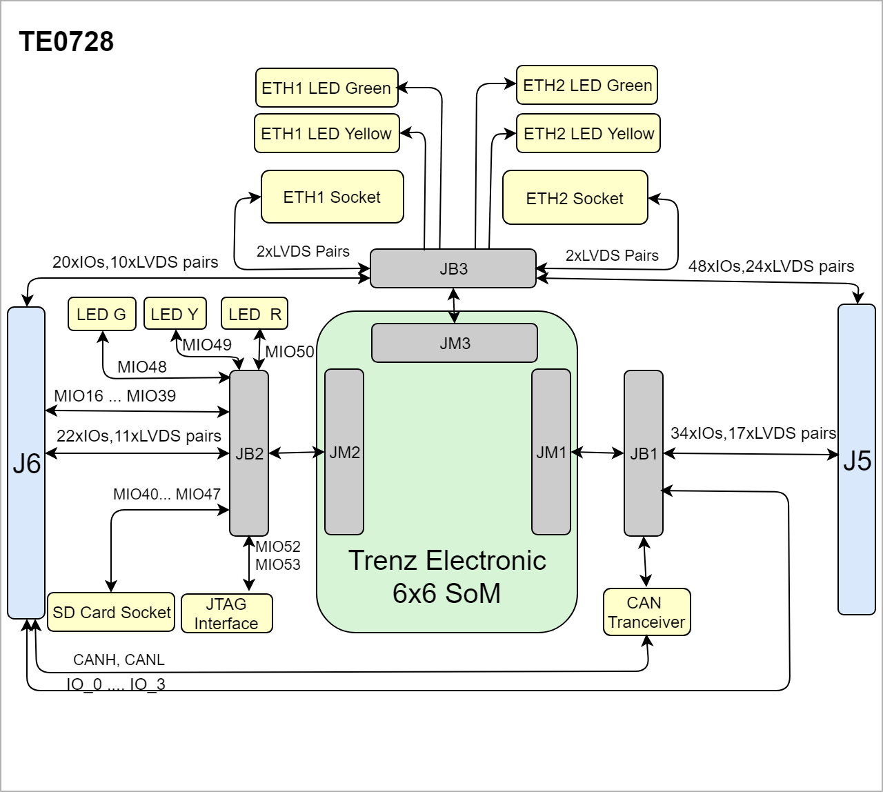
The Trenz Electronic TE0728 TEB0728 Carrier Board provides functionalities for testing, evaluation and development purposes of company's 6 x 6 cm SoMs. The Carrier Board is equipped with various components and connectors for different configuration setups and needs. The interfaces of the SoM's functional units and PL I/O-banks are connected via board-to-board connectors to the Carrier Board's components and connectors for easy user access.. See "6 x 6 SoM" Carriers" page for more information about supported 6 x 6 cm SoMs.
Refer to http://trenz.org/te0728TEB0728-info for the current online version of this manual and other available documentation.
Key Features
- Samtec Tiger Eye Terminal Socket ( 80 pins, 2 rows)
- Micro SD card socket
- 3 User LEDs, Red, Yellow, Green
- Two RJ45 Gigabit Ethernet socket
- Trenz 6x6 module connector strips (3 x Samtec Tiger Eye series connectors)
- Barrel Jack for 12V 5V power supply
- One user push button
Block Diagram
| Scroll Title |
|---|
| anchor | Figure_OV_BD |
|---|
| title | TE0728 TEB0728 block diagram |
|---|
|
| Scroll Ignore |
|---|
| draw.io Diagram |
|---|
| border | truefalse |
|---|
| viewerToolbar | true |
|---|
| |
|---|
| fitWindow | false |
|---|
| diagramDisplayName | |
|---|
| lbox | true |
|---|
| revision | 17 |
|---|
| diagramName | TE0728_BD1 |
|---|
| simpleViewer | false |
|---|
| width | |
|---|
| links | auto |
|---|
| tbstylediagramWidth | 640hidden |
|---|
| revisiondiagramWidth | 1641 |
|---|
|
|
|
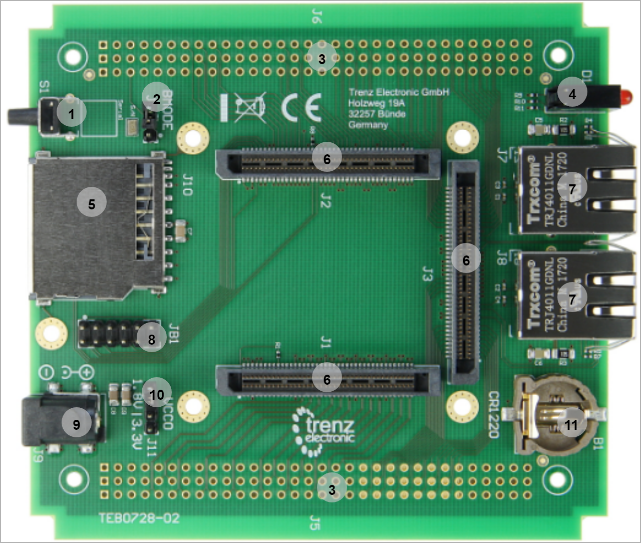
Main Components
| Page properties |
|---|
|
Notes : - Picture of the PCB (top and bottom side) with labels of important components
- Add List below
|
...
| Scroll Title |
|---|
| anchor | Figure_OV_MC |
|---|
| title | TE0728 TEB0728 main components |
|---|
|
| Scroll Ignore |
|---|
| draw.io Diagram |
|---|
| border | truefalse |
|---|
| viewerToolbar | true |
|---|
| |
|---|
| fitWindow | false |
|---|
| diagramDisplayName | |
|---|
| lbox | true |
|---|
| revision | 821 |
|---|
| diagramName | TE0728_MC |
|---|
| simpleViewer | false |
|---|
| width | |
|---|
| links | auto |
|---|
| tbstyle | hidden |
|---|
| diagramWidth | 616642 |
|---|
|
|
| Scroll Only |
|---|
|
|
- User push-button, S1
- Jumper (Boot Mode), J4
- External connector (VG96) placeholder, J5 / J6
- LEDs , D1
- SD
- Board to Board Connector, J1-J2-J3
- LEDs , D1
- CR1220 Backup-Battery holder, B1
- SD Card Connector, J10
- Board to Board Connector, J1-J2-J3
- RJ45 Gigabit Ethernet connector, J7-J8
- User push-button, S1
- Jumper, J4
- XMOD JTAG- / UART-header, JB1
- Barrel jack for 5V power supply, J9
- Jumper Jumper(VCCIO_13), J11
- External connector (VG96) placeholder, J5 / J6
- JTAG interface baseCR1220 Backup-Battery holder, B1
Initial Delivery State
There is no hardware component to be programmed on teh the carrier.
| Scroll Title |
|---|
| anchor | Table_OV_IDS |
|---|
| title | Initial delivery state of programmable devices on the module |
|---|
|
| Scroll Table Layout |
|---|
| orientation | portrait |
|---|
| sortDirection | ASC |
|---|
| repeatTableHeaders | default |
|---|
| style | |
|---|
| widths | |
|---|
| sortByColumn | 1 |
|---|
| sortEnabled | false |
|---|
| cellHighlighting | true |
|---|
|
Storage device name | Content | Notes |
|---|
|
...
Configuration Signals
| Page properties |
|---|
|
- Overview of Boot Mode, Reset, Enables,
|
Boot Process
| Scroll Title |
|---|
| anchor | Table_OV_BP |
|---|
| title | Boot process. |
|---|
|
| Scroll Table Layout |
|---|
| orientation | portrait |
|---|
| sortDirection | ASC |
|---|
| repeatTableHeaders | default |
|---|
| style | |
|---|
| widths | |
|---|
| sortByColumn | 1 |
|---|
| sortEnabled | false |
|---|
| cellHighlighting | true |
|---|
|
Signal | Designator | B2B | Jumper | Boot Mode |
|---|
Boot_R | J4 | J2-11 | Open | QSPI | | Short | SD Card |
|
Reset Process
There is a user push button which is used for RESET signal.
| Scroll Title |
|---|
| anchor | Table_OV_BP |
|---|
| title | Reset process. |
|---|
|
| Scroll Table Layout |
|---|
| orientation | portrait |
|---|
| sortDirection | ASC |
|---|
| repeatTableHeaders | default |
|---|
| style | |
|---|
| widths | |
|---|
| sortByColumn | 1 |
|---|
| sortEnabled | false |
|---|
| cellHighlighting | true |
|---|
|
Signal | Designator | B2B | Active Level |
|---|
RESET | S1 | J2-7 | Active High |
|
Signals, Interfaces and Pins
| Page properties |
|---|
|
Notes : - For carrier or stand-alone boards use subsection for every connector type (add designator on description, not on the subsection title), for example:
- For modules which needs carrier use only classes and refer to B2B connector if more than one is used, for example
|
Board to Board (B2B) I/Os
Number of I/O signals FPGA bank numbers connected to the B2B connectors:
| Scroll Title |
|---|
| anchor | Table_SIP_B2B |
|---|
| title | General overview of PL I/O signals and SoM's interfaces connected to the B2B connectors. |
|---|
|
| Scroll Table Layout |
|---|
| orientation | portrait |
|---|
| sortDirection | ASC |
|---|
| repeatTableHeaders | default |
|---|
| style | |
|---|
| widths | |
|---|
| sortByColumn | 1 |
|---|
| sortEnabled | false |
|---|
| cellHighlighting | true |
|---|
|
| B2B Connector | Interfaces | Number of I/O | Notes |
|---|
J1
| User I/O | 48 singel ended, 24 differential | Connected to Bank 13 | | 4 Single ended | MIO10 |
-| ...13 | | CANH , CANL | 2 single ended | MIO8, MIO9 | J2
| User I/O | 22 singel ended, 11 differential |
| | 38 single ended | MIO16 |
-| ...53 | | SoM Control Signals | 5 | RESET, RST_OUT, BOOT_R, | | JTAG Interface | 4 | TCK , TDO, TDI, TMS | J3
| User I/O | 20 Single ended, 10 differential
| Connected to Bank 35 | | 34 single ended, 17 differential | Connected to Bankd 33 | | Ethernet 1 | 4 single ended, 2 differential | ETH_CTREF , ETH_TD+, ETH_TD- , ETH_RD+, ETH_RD-, ETH_LED1, ETH_LED2, ETH_LED3 | | Ethernet 2 | 4 single ended, 2 differential | ETH_CTREF , ETH_TD+, ETH_TD- , ETH_RD+, ETH_RD-, ETH_LED1, ETH_LED2, ETH_LED3 |
|
On-board Connector
There are two pin placeholder on the board, J5-J6.
| Scroll Title |
|---|
| anchor | Table_SIP_B2BOnB |
|---|
| title | General PL I/O to B2B information about On-board connectors information |
|---|
|
| Scroll Table Layout |
|---|
| orientation | portrait |
|---|
| sortDirection | ASC |
|---|
| repeatTableHeaders | default |
|---|
| style | |
|---|
| widths | |
|---|
| sortByColumn | 1 |
|---|
| sortEnabled | false |
|---|
| cellHighlighting | true |
|---|
|
| B2B VGA96 Vertical Connector | Interfaces | Number of I/O | Notes |
|---|
J5
| User I/O | 48 singel ended, 24 differential | Connected to Bank 13 | | 34 single ended, 17 differential | Connected to Bank 33 | J6
| User I/O | 42 singel ended, 21 differential |
| | 27 single ended | MIO16... MIO39 + MIO 51-MIO51...53 | | 4 single ended | MIO10-...13 | | SoM Control Signals | 3 | RESET, RST_OUT, BOOT_R | | JTAG Interface | 4 | TCK , TDO, TDI, TMS | CANH , CANL | 2 single ended | MIO8, MIO9 |
|
JTAG Interface Base
JTAG access to the TE0728 TEB0728 Trenz Module module is available through B2B connector J2. JTAG Programmer TE0790_02 is provided by Trenz Electronic, More information is available here.
| Scroll Title |
|---|
| anchor | Table_SIP_JTG |
|---|
| title | JTAG interface Base |
|---|
|
| Scroll Table Layout |
|---|
| orientation | portrait |
|---|
| sortDirection | ASC |
|---|
| repeatTableHeaders | default |
|---|
| style | |
|---|
| widths | |
|---|
| sortByColumn | 1 |
|---|
| sortEnabled | false |
|---|
| cellHighlighting | true |
|---|
|
Connected to | B2B Pin | XMOD Header JB1 | Note |
|---|
| A |
MIO52 | J2-15 | JB1-3 | UART Txd - input | | B |
MIO53 | J2-16 | JB1-7 | UART Rxd - Output | | C |
TMS | JTAG interface signalTDI interface signalTDO | JTAG interface signalTCKJTAG interface signal | |
JTAG mode
The DIP-switch S2 on JTAG interface is connected to JTAGEN.
| JB1-12 | JTAG-TCK | | G | J2-7 | JB1-11 | RESET will be connected to Push Button on JTAG Programmer | | 3.3V | - | JB1-5 | connected to GND | | VIO | J2-2/4 | JB1-6 | VIO is connected to 3.3V which is supplied by carrier |
|
SD Card Socket
Power supply voltage for SD card holder is 3.3V.
| Scroll Title |
|---|
| anchor | Table_OBP |
|---|
| title | On board peripherals |
|---|
|
|
| Scroll Title |
|---|
| anchor | Table_SIP_JTG_Mode |
|---|
| title | JTAG Mode |
|---|
|
| Scroll Table Layout |
|---|
| orientation | portrait |
|---|
| sortDirection | ASC |
|---|
| repeatTableHeaders | default |
|---|
| style | |
|---|
| widths | |
|---|
| sortByColumn | 1 |
|---|
| sortEnabled | false |
|---|
| cellHighlighting | true |
|---|
|
| S2Signals | ONB2B | OFFNotes |
|---|
Default| CMD | DescriptionJ2-29 | | 1 | Normal mode | Adapter board CPLD update mode | ON | Update Mode JTAG access to SC CPLD only | | 2 | Do not use (illegal setting) | Normal mode | OFF | Must be in OFF state always. | | 3 | VIO connected to 3.3V | Power VIO from pin header J2 | OFF | User I/O Voltage | | 4 | Power 3.3V from USB | Power 3.3V from pin header J2 | OFF | Power on-board peripherals (FTDI chip & SC CPLD, ...) |
|
...
| Page properties |
|---|
|
Notes : - add subsection for every component which is important for design, for example:
- Two 100 Mbit Ethernet Transciever PHY
- USB PHY
- Programmable Clock Generator
- Oscillators
- eMMCs
- RTC
- FTDI
- ...
- DIP-Switches
- Buttons
- LEDs
|
SD Card Socket
VDD for SD card holder is 3.3V.
...
| anchor | Table_OBP |
|---|
| title | On board peripherals |
|---|
...
RJ45 Connector
...
| anchor | Table_OBP_SPI |
|---|
| title | Quad SPI interface MIOs and pins |
|---|
...
| | CLK | J2-34 |
| | DAT0 | J2-37 |
| | DAT1 | J2-40 |
| | DAT2 | J2-32 |
| | CD/DAT3 | J2-31 |
| | CD | J2-35 |
| | WP | J2-33 |
|
|
RJ45 Connector
Both Ethernet sockets,ETH1 and ETH2, are connected to the Board to Board (B2B) J3 on the carrier.
Push button
| Scroll Title |
|---|
| anchor | Table_OBP_Push_ButtonETH |
|---|
| title | On-board push buttonEthernet Connections to B2B Connectors |
|---|
|
| Scroll Table Layout |
|---|
| orientation | portrait |
|---|
| sortDirection | ASC |
|---|
| repeatTableHeaders | default |
|---|
| style | |
|---|
| widths | |
|---|
| sortByColumn | 1 |
|---|
| sortEnabled | false |
|---|
| cellHighlighting | true |
|---|
|
|
| Designator | Connected to | B2B | Active Level | Note |
|---|
| S1 | RESET | J2-7 | Active high | General Input RESET |
Jumpers
...
| anchor | Table_OBP_Jumpers |
|---|
| title | On-board Jumpers |
|---|
...
| Signal | ETH1 | ETH2 | Notes |
|---|
| ETH_TD+ | J3-58 | J3-28 | Transfer | | ETH_TD- | J3-56 | J3-26 |
| | ETH_RD+ | J3_52 | J3-22 | Receive | | ETH_RD- | J3-50 | J3-20 |
| | ETH_CTREF | J3_57 | J3-25 |
| | ETH_LED1 | J3-55 | J3-23 | Yellow LED- Activity | | ETH_LED3 | J3-51 | J3-19 | Green Green- Link |
|
On-board Peripherals
| Page properties |
|---|
|
Notes : - add subsection for every component which is important for design, for example:
- Two 100 Mbit Ethernet Transciever PHY
- USB PHY
- Programmable Clock Generator
- Oscillators
- eMMCs
- RTC
- FTDI
- ...
- DIP-Switches
- Buttons
- LEDs
|
Push button
...
| Scroll Title |
|---|
| anchor | Table_OBP_LEDPush_Button |
|---|
| title | On-board LEDspush button |
|---|
|
| Scroll Table Layout |
|---|
| orientation | portrait |
|---|
| sortDirection | ASC |
|---|
| repeatTableHeaders | default |
|---|
| style | |
|---|
| widths | |
|---|
| sortByColumn | 1 |
|---|
| sortEnabled | false |
|---|
| cellHighlighting | true |
|---|
|
| Color | | Connected to | B2B | Active Level | Note |
|---|
D1Red | MIO4830Active high | D1-B | Yellow | MIO49 | J2-38 | Active high | D1-C | Green | MIO50 | J2-36 | Active high | |
...
| 7 | Active high | General Input RESET |
|
Jumpers
Power Supply
Single 12V power supply with minimum current capability of 3.5A is recommended to operate the board.
...
| Scroll Title |
|---|
| anchor | Table_PWROBP_PCJumpers |
|---|
| title | Power ConsumptionOn-board Jumpers |
|---|
|
| Scroll Table Layout |
|---|
| orientation | portrait |
|---|
| sortDirection | ASC |
|---|
| repeatTableHeaders | default |
|---|
| style | |
|---|
| widths | |
|---|
| sortByColumn | 1 |
|---|
| sortEnabled | false |
|---|
| cellHighlighting | true |
|---|
|
|
| Power Input Pin | Typical Current |
|---|
| VIN | TBD* |
| VBATT | TBD* |
...
Power Distribution Dependencies
...
| anchor | Figure_PWR_PD |
|---|
| title | Power Distribution |
|---|
...
Power-On Sequence
...
| Designator | Connected to | B2B | Note |
|---|
| J4 | Boot_R | J2-11 | Open: QSPI | | Short: SD Card |
|
| Scroll Title |
|---|
| anchor | FigureTable_PWROBP_PSJumpers |
|---|
| title | Power SequencyOn-board Jumpers |
|---|
|
ignore| draw.io Diagram |
|---|
|
| border | true |
|---|
| viewerToolbar | true |
|---|
| fitWindow | false |
|---|
diagramDisplayName | | lbox | true |
|---|
| revision | 1 |
|---|
| diagramName | TE0728_PWR_PS |
|---|
| simpleViewer | false |
|---|
| width | 640 |
|---|
| links | auto |
|---|
| tbstyle | top |
|---|
| diagramWidth | 641 |
|---|
| Scroll Only |
|---|
 Image Removed Image Removed
|
...
| tablelayout |
|---|
| orientation | portrait |
|---|
| sortDirection | ASC |
|---|
| repeatTableHeaders | default |
|---|
| style | |
|---|
| widths | |
|---|
| sortByColumn | 1 |
|---|
| sortEnabled | false |
|---|
| cellHighlighting | true |
|---|
|
| Designator | Connected to | Voltage | Note |
|---|
| J11 | VCCIO_13 | 3.3 V | Pin 1 and the middle pin are connected | | 1.8 V | Pin 3 and the middle pin are connected |
|
LEDs
| Scroll Title |
|---|
| anchor | Table_PWROBP_PRLED |
|---|
| title | Module power rails.On-board LEDs |
|---|
|
| Scroll Table Layout |
|---|
| orientation | portrait |
|---|
| sortDirection | ASC |
|---|
| repeatTableHeaders | default |
|---|
| style | |
|---|
| widths | |
|---|
| sortByColumn | 1 |
|---|
| sortEnabled | false |
|---|
| cellHighlighting | true |
|---|
|
|
| Power Rail Name | B2B Connector | Direction | Notes |
|---|
VIN | J1-1, J1-3 | Input | | VBAT | J2-1 | Input | Battery for RTC |
| VCCO_13 | J1-39 | Input | Jumper(J11) connects VCCO_13 to 3.3v or 1.8v |
...
| false |
|---|
| cellHighlighting | true |
|---|
|
| Designator | Color | B2B | Active Level | Note |
|---|
| D1-A | Red | J2-30 | Active high |
| | D1-B | Yellow | J2-38 | Active high |
| | D1-C | Green | J2-36 | Active high |
|
|
Power and Power-On Sequence
Power Supply
| Note |
|---|
| No power supply protection circuit on the carrier, module will be powered directly |
Single 5V power supply with minimum current capability of 2.5A is recommended to operate the board.
- 5V VIN (inner)
GND (outer)
| Scroll Title |
|---|
| anchor | Figure_pwr_connector |
|---|
| title | Power Connector |
|---|
|
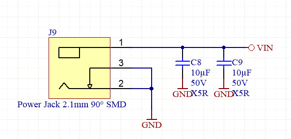 Image Added Image Added
|
Power Consumption
| Scroll Title |
|---|
| anchor | Table_PWR_PRPC |
|---|
| title | Carrier Power Rails.Consumption |
|---|
|
| Scroll Table Layout |
|---|
| orientation | portrait |
|---|
| sortDirection | ASC |
|---|
| repeatTableHeaders | default |
|---|
| style | |
|---|
| widths | |
|---|
| sortByColumn | 1 |
|---|
| sortEnabled | false |
|---|
| cellHighlighting | true | | true |
|---|
|
| Power Input Pin | Typical Current |
|---|
| Module Connector (B2B) Designator | VCC / VCCIO | Direction | Pins | Notes |
|---|
JB1 | | VIN | In | 1,3 | Up to 12V carrier supply voltage | | 3.3V | In | 19 | PL IO-bank VCCIO | | VCCO_13 | In | 39 | 1.8V or 3.3V | | JB2 | 3.3V | In | 2, 4 | 3.3V module supply voltage | | 1.8V | In | 5 | PL IO-bank VCCIO | | VBATT | In | 1 | RTC buffer voltage | | JB3 | - | - | - | - |
|
| Scroll Title |
|---|
|
* TBD - To Be Determined
Power Rails
| Scroll Title |
|---|
| anchor | Table_PWR_PR |
|---|
| title | Carrier Power Rails. |
|---|
|
| Scroll Table Layout |
|---|
| orientation | portrait |
|---|
| sortDirection | ASC |
|---|
| repeatTableHeaders | default |
|---|
| style | |
|---|
| widths | |
|---|
| sortByColumn | 1 |
|---|
| sortEnabled | false |
|---|
| cellHighlighting | true |
|---|
|
| Module Connector (B2B) Designator | VCC / VCCIO | Direction | Pins | Notes |
|---|
| JB1 | VIN | Output | 1, 3 | Up to 12V carrier supply voltage | | 3.3V | Input | 19 | PL IO-bank VCCIO | | VCCO_13 | Output | 39 | 1.8V or 3.3V over jumper | | JB2 | 3.3V | Input | 2, 4 | 3.3V module supply voltage | | 1.8V | Input | 5 | PL IO-bank VCCIO | | VBATT | Output | 1 | RTC buffer voltage | | JB3 | - | - | - | - |
|
| anchor | Table_PWR_PR |
|---|
| title | Carrier Power Rails. |
|---|
|
| Scroll Table Layout |
|---|
|
| orientation | portrait |
|---|
| sortDirection | ASC |
|---|
| repeatTableHeaders | default |
|---|
style | widths | | sortByColumn | 1 |
|---|
| sortEnabled | false |
|---|
| cellHighlighting | true |
|---|
| On-board Connector Designator | VCC / VCCIO | Direction | Pins | Notes |
|---|
Ja5 | VIN | In | A1,A2 | Up to 12V carrier supply voltage
Board to Board Connectors
modules use two or three Samtec Micro Tiger Eye Connector on the bottom side....
| SoM TEM and SEM B2B Connectors | | 6 x 6 SoM TEM and SEM B2B Connectors |
|---|
|
Absolute Maximum Ratings
| Scroll Title |
|---|
| anchor | Table_TS_AMR |
|---|
| title | Module absolute maximum ratings. |
|---|
|
| Scroll Table Layout |
|---|
| orientation | portrait |
|---|
| sortDirection | ASC |
|---|
| repeatTableHeaders | default |
|---|
| style | |
|---|
| widths | |
|---|
| sortByColumn | 1 |
|---|
| sortEnabled | false |
|---|
| cellHighlighting | true |
|---|
|
| Note | VIN supply voltage | 5 | 12 | | Note |
|---|
| VIN supply voltage | -- | -- | V | - Connected directly to the module power supply, see Module TRM
| | Storage Temperature | -25 | +85 | °C |
V
|
Recommended Operating Conditions
Recommended Temprature: -40°C to +100°C.
Operating temperature range depends also on customer design and cooling solution. Please contact us for options.
| Scroll Title |
|---|
| anchor | Table_TS_ROC |
|---|
| title | Recommended operating conditions. |
|---|
|
| Scroll Table Layout |
|---|
| orientation | portrait |
|---|
| sortDirection | ASC |
|---|
| repeatTableHeaders | default |
|---|
| style | |
|---|
| widths | |
|---|
| sortByColumn | 1 |
|---|
| sortEnabled | false |
|---|
| cellHighlighting | true |
|---|
|
| Parameter | Min | Max | Units | Note |
|---|
| VIN supply voltage |
512| -- | V | - Connected directly to the module power supply, see Module TRM
- 5V recommended for usage with TE0728
| | Operating Temperature | -25 | +85 | °C |
|
|
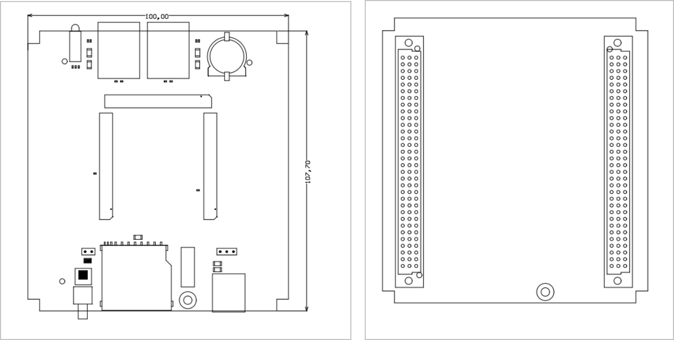
Physical Dimensions
Module size: 60 mm × 60 100 mm × 107.7 mm. Please download the assembly diagram for exact numbers.
Mating height with standard connectors: 7 mm.
PCB thickness: 1.6 mm.
| Scroll Title |
|---|
| anchor | Figure_TS_PD |
|---|
| title | Physical Dimension |
|---|
|
| Scroll Ignore |
|---|
| draw.io Diagram |
|---|
| border | true |
|---|
| viewerToolbar | true |
|---|
| |
|---|
| fitWindow | false |
|---|
| diagramDisplayName | |
|---|
| lbox | true |
|---|
| revision |
|---|
|
|
1| 8 | | diagramName | Figure_TS_PD |
|---|
| simpleViewer | false |
|---|
| width |
|---|
|
|
640top1761
| Scroll Only |
|---|
| scroll-pdf | true |
|---|
| scroll-office | true |
|---|
| scroll-chm | true |
|---|
| scroll-docbook | true |
|---|
| scroll-eclipsehelp | true |
|---|
| scroll-epub | true |
|---|
| scroll-html | true |
|---|
| 
|
|
Currently Offered Variants
...
...
| Scroll Title |
|---|
| anchor | Table_VCP_SO |
|---|
| title | Trenz Electronic Shop Overview |
|---|
|
| Scroll Table Layout |
|---|
| orientation | portrait |
|---|
| sortDirection | ASC |
|---|
| repeatTableHeaders | default |
|---|
| style | |
|---|
| widths | |
|---|
| sortByColumn | 1 |
|---|
| sortEnabled | false |
|---|
| cellHighlighting | true |
|---|
|
|
Revision History
Hardware Revision History
| Scroll Title |
|---|
| anchor | Table_RH_HRH |
|---|
| title | Hardware Revision History |
|---|
|
| Scroll Table Layout |
|---|
| orientation | portrait |
|---|
| sortDirection | ASC |
|---|
| repeatTableHeaders | default |
|---|
| style | |
|---|
| widths | |
|---|
| sortByColumn | 1 |
|---|
| sortEnabled | false |
|---|
| cellHighlighting | true |
|---|
|
| Date | Revision | Changes |
|---|
| 2018-07-18 | 02 | - changed value R1
- changed magjack connectors J7, J8
- changed 2.1mm power jack THT on SMD
- magjack connectors: pin8 connected to frame (shassis ground)
- lib component update
- added thermal bias to mounting holes
- added visual serial number
- changed 2.1mm power jack THT on SMD
- added 2 x 10uF to VIN
| | 2016-11-02 | 01 | |
| Date | Revision | Note | PCN | Documentation Link |
|---|
- | 01 | Prototypes | - |
|
Hardware revision number is printed on the PCB board next to the module model number separated by the dash.
Document Change History
| Page properties |
|---|
|
- Note this list must be only updated, if the document is online on public doc!
- It's semi automatically, so do following
Add new row below first Copy "Page Information Macro(date)" Macro-Preview, Metadata Version number, Author Name and description to the empty row. Important Revision number must be the same as the Wiki document revision number Update Metadata = "Page Information Macro (current-version)" Preview+1 and add Author and change description. --> this point is will be deleted on newer pdf PDF export template - Metadata is only used of compatibility of older exports
|
...
| Scroll Title |
|---|
| anchor | Table_RH_DCH |
|---|
| title | Document change history. |
|---|
|
| Scroll Table Layout |
|---|
| orientation | portrait |
|---|
| sortDirection | ASC |
|---|
| repeatTableHeaders | default |
|---|
| style | |
|---|
| widths | |
|---|
| sortByColumn | 1 |
|---|
| sortEnabled | false |
|---|
| cellHighlighting | true |
|---|
|
| Date | Revision | Contributor | Description |
|---|
| Page info |
|---|
| infoType | Modified date |
|---|
| dateFormat | yyyy-MM-dd |
|---|
| type | Flat |
|---|
|
| | Page info |
|---|
| infoType | Current version |
|---|
| prefix | v. |
|---|
| type | Flat |
|---|
| showVersions | false |
|---|
|
| | Page info |
|---|
| infoType | Modified by |
|---|
| type | Flat |
|---|
| showVersions | false |
|---|
|
change list | typo table title - power rail section
| | 2019-6-25 | v.132 | Pedram Babakhani | | -- | all | | Page info |
|---|
| infoType | Modified users |
|---|
| type | Flat |
|---|
| showVersions | false |
|---|
|
| |
|
Disclaimer
| Include Page |
|---|
| IN:Legal Notices |
|---|
| IN:Legal Notices |
|---|
|
...