...
* TBD - To Be Determined
Power on Sequence
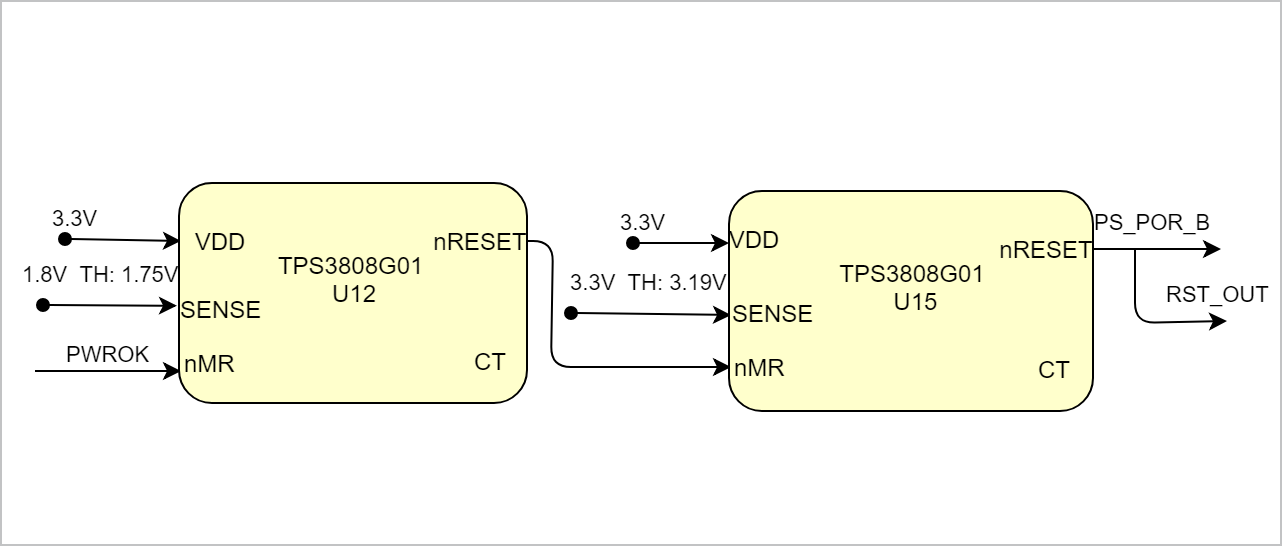
The PS and PL power supplies are fully independent. The recommended power-on sequence is VCCPINT, VCCPAUX and VCCPLL together, then the PS VCCO supplies (VCCO_MIO0, VCCO_MIO1, and VCCO_DDR) to achieve minimum current draw and ensure that the I/Os are 3-stated at power-on. TE07028 SoM meets the recommended criteria to power up the Xilinx Zynq properly by keeping a specific sequence of enabling the on-board DC-DC converters and regulators dedicated to the particular functional units of the Zynq chip and powering up the on-board voltages. When the U8 and U9 generates PWRGD signal, it turns on the U4 which generates PWRGD_3.3V, it turns on the U6 and it generates PWROK signal which is connected to MR. Whenever the supply voltage for U12 drops down below the threshold it resets the system. Actually it resets the system when all regulators are working.
| Scroll Title |
|---|
| anchor | Figure_PWR_PS |
|---|
| title | Power On Sequence |
|---|
|
| Scroll Ignore |
|---|
| scroll-pdf | true |
|---|
| scroll-office | true |
|---|
| scroll-chm | true |
|---|
| scroll-docbook | true |
|---|
| scroll-eclipsehelp | true |
|---|
| scroll-epub | true |
|---|
| scroll-html | true |
|---|
| | draw.io Diagram |
|---|
| border | false |
|---|
| viewerToolbar | true |
|---|
| |
|---|
| fitWindow | false |
|---|
| diagramDisplayName | |
|---|
| lbox | false |
|---|
| revision | 6 |
|---|
| diagramName | Figure_PWR_PS |
|---|
| simpleViewer | false |
|---|
| width | |
|---|
| links | auto |
|---|
| tbstyle | hidden |
|---|
| diagramWidth | 641 |
|---|
|
|
| Scroll Only |
|---|
| scroll-pdf | true |
|---|
| scroll-office | true |
|---|
| scroll-chm | true |
|---|
| scroll-docbook | true |
|---|
| scroll-eclipsehelp | true |
|---|
| scroll-epub | true |
|---|
| scroll-html | true |
|---|
| 
|
|
...
The microprocessor supervisory circuits monitor system voltages asserting an open-drain RESET signal when the SENSE voltage drops below a preset threshold or when the manual reset (MR) pin drops to a logic low. The RESET output remains low for the user adjustable delay time after the SENSE voltage and MR return above their thresholds. Datasheet is available in Texas Instruments website.
When the U8 and U9 generates PWRGD signal, it turns on the U4 which generates PWRGD_3.3V, it turns on the U6 and it generates PWROK signal which is connected to MR. Whenever the supply voltage for U12 drops down below the threshold it resets the system. Actually it resets the system when all regulators are working.
Power Rails
| Scroll Title |
|---|
| anchor | Table_PWR_PR |
|---|
| title | Module power rails. |
|---|
|
| Scroll Table Layout |
|---|
| orientation | portrait |
|---|
| sortDirection | ASC |
|---|
| repeatTableHeaders | default |
|---|
| style | |
|---|
| widths | |
|---|
| sortByColumn | 1 |
|---|
| sortEnabled | false |
|---|
| cellHighlighting | true |
|---|
|
B2B Name | B2B JM1 Pin | B2B JM2 Pin | B2B JM3 Pin | Direction | Notes |
|---|
| VIN | 1,3 | - | - | Input | Supply voltage from carrier board. | | VCCO_13 | 39 | - | - | I/O |
| | VBATT | - | 1 | - | Output | RTC Supply voltage | | 3.3V | 19 | 4 | 25,57 | Output | Internal 3.3V voltage level. | | VMIO | - | 2 |
| Input | 3.3V from carrier | 1.8V | - | 5 | - | Output | Internal 1.8V voltage level. |
|
...
| Scroll Title |
|---|
| anchor | Table_TS_AMR_PL |
|---|
| title | PL absolute maximum ratings |
|---|
|
| Scroll Table Layout |
|---|
| orientation | portrait |
|---|
| sortDirection | ASC |
|---|
| repeatTableHeaders | default |
|---|
| style | |
|---|
| widths | |
|---|
| sortByColumn | 1 |
|---|
| sortEnabled | false |
|---|
| cellHighlighting | true |
|---|
|
| Symbols | Description | Min | Max | Unit |
|---|
| VCCINT | PL internal logic supply voltage | -0.5 | 1.1 | V | | VCCPAUX | PL auxiliary supply voltage | -0.5 | 2.0 | V | | VCCPLL | PL PLL supply | -0.5 | 1.1 | V | | VPREF | PL input reference voltage | -0.5 | 2.0 | V | | VCCO | PL supply voltage for HR I/O banks | -0.5 | 3.6 | V | | VIN | I/O input voltage for HR I/O banks | 1.71 | 3.45 | V |
|
Recommended Operating
...
Conditionse
| Scroll Title |
|---|
| anchor | Table_TS_ROC |
|---|
| title | Recommended operating conditions |
|---|
|
| Scroll Table Layout |
|---|
| orientation | portrait |
|---|
| sortDirection | ASC |
|---|
| repeatTableHeaders | default |
|---|
| style | |
|---|
| widths | |
|---|
| sortByColumn | 1 |
|---|
| sortEnabled | false |
|---|
| cellHighlighting | true |
|---|
|
| Parameter | Min | Max | Units | Reference Document |
|---|
| VIN supply voltage | 3.5 | 60 | V | TPS54260-Q1 datasheets. | | Supply voltage for PS MIO banks | 1.71 | 3.465 | V | See Xilinx DS187 datasheet. | | I/O input voltage for PS MIO banks | -0.2 | VCCO_MIO + 0.20 | V | See Xilinx DS187 datasheet. | | Supply voltage for PS DDR | 1.14 | 1.89 | V | See Xilinx DS187 datasheet. | | I/O input voltage for PS DDR | -0.20 | VCCO_DDR + 0.20 | V | See Xilinx DS187 datasheet. | | Supply voltage for HR I/Os banks | 1.14 | 3.465 | V | See Xilinx DS187 datasheet. | | I/O input voltage for HR I/O banks | -0.20 | VCCIO + 0.20 | V | See Xilinx DS187 datasheet. | | Storage Temperature | -4540 | +125 | °C | See Xilinx DS187 datasheet. |
|
Temprature Operating range: -40°C to +85°C105°C.
Operating temperature range depends also on customer design and cooling solution. Please contact us for options.
...