...
| Scroll Title |
|---|
| anchor | Figure_OV_BD |
|---|
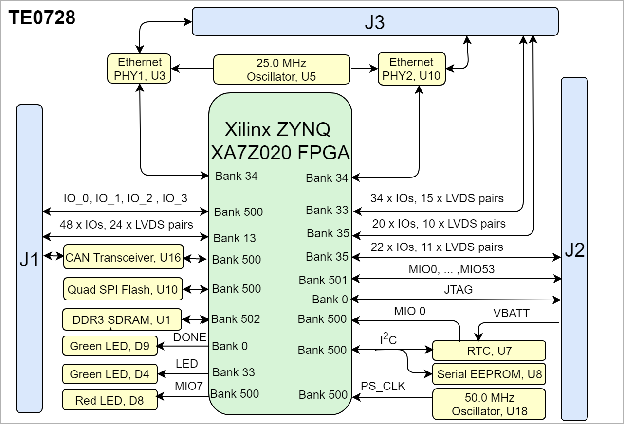
| title | TE0728 block diagram |
|---|
|
| Scroll Ignore |
|---|
| draw.io Diagram |
|---|
| border | false |
|---|
| viewerToolbar | true |
|---|
| |
|---|
| fitWindow | false |
|---|
| diagramDisplayName | |
|---|
| lbox | true |
|---|
| revision | 1819 |
|---|
| diagramName | TE0728_OV_BD |
|---|
| simpleViewer | false |
|---|
| width | |
|---|
| links | auto |
|---|
| tbstyle | hidden |
|---|
| diagramWidth | 641 |
|---|
|
|
| Scroll Only |
|---|
|
|
...
| Scroll Title |
|---|
| anchor | Figure_OV_MC |
|---|
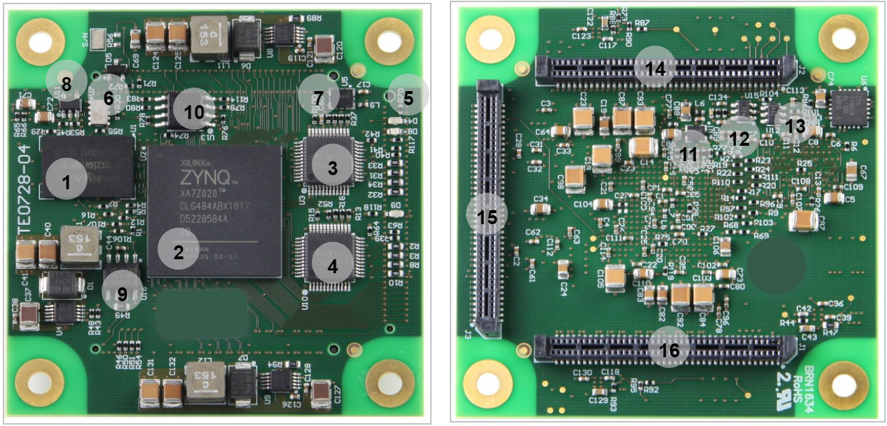
| title | TE0728 main components |
|---|
|
| Scroll Ignore |
|---|
| draw.io Diagram |
|---|
| border | false |
|---|
| viewerToolbar | true |
|---|
| |
|---|
| fitWindow | false |
|---|
| diagramDisplayName | |
|---|
| lbox | false |
|---|
| revision | 4849 |
|---|
| diagramName | TE0728_MC2 |
|---|
| simpleViewer | true |
|---|
| width | |
|---|
| links | auto |
|---|
| tbstyle | hidden |
|---|
| diagramWidth | 633 |
|---|
|
|
| Scroll Only |
|---|
| scroll-pdf | true |
|---|
| scroll-office | true |
|---|
| scroll-chm | true |
|---|
| scroll-docbook | true |
|---|
| scroll-eclipsehelp | true |
|---|
| scroll-epub | true |
|---|
| scroll-html | true |
|---|
| 
|
|
...
Board to Board (B2B) I/Os
TE0728 Module has 3 B2B connectors and every connector has 80 pins (2 row, 40 pins).
FPGA bank number and number of I/O signals connected to the B2B connector:
...
| Scroll Title |
|---|
| anchor | Table_OBP_MIOs |
|---|
| title | MIOs pins |
|---|
|
| Scroll Table Layout |
|---|
| orientation | portrait |
|---|
| sortDirection | ASC |
|---|
| repeatTableHeaders | default |
|---|
| style | |
|---|
| widths | |
|---|
| sortByColumn | 1 |
|---|
| sortEnabled | false |
|---|
| cellHighlighting | true |
|---|
|
| MIO Pin | Connected to | B2B | Notes |
|---|
| MIO0 | MIO0 | - | RTC interrupt | | MIO1...MIO6 | SPI_CS , SPI_DQ0... SPI_DQ3 SPI_SCK | - | SPI Flash | | MIO7 | LED RED | - | LED | | MIO8/MIO9 | Tx/Rx | - | CAN Transceiver | | MIO10...MIO13 | IO_0 ... IO_3 | J1 | GPIO | | MIO14/MIO15 | SCL/SDA | - | I2C | | MIO16...MIO27 | - | J2 | GPIO | | MIO28...MIO39 | Tx_clk, Txd0...Txd3, Tx_ctl Rx_clk, Rxd0...Rxd3, Rx_ctl | J2 | ETH Socket on carrier TEB0728 | | MIO40...MIO48 | CLK, Cmd, Data0...Data3, wp, cd | J2 | SD | | MIO48 | PS_MIO48_501 | J2 | LED Red on Carrier | | MIO49 | PS_MIO49_501 | J2 | LED Yellow on Carrier | | MIO50 | PS_MIO49_501 | J2 | LED Green on Carrier | | MIO51 | PS_MIO51_501 | J2 | GPIO | | MIO52/MIO53 | UART_Txd / UART_Rxd | J2 | UART transfer/recieve |
|
...
| Scroll Title |
|---|
| anchor | Figure_PWR_PD |
|---|
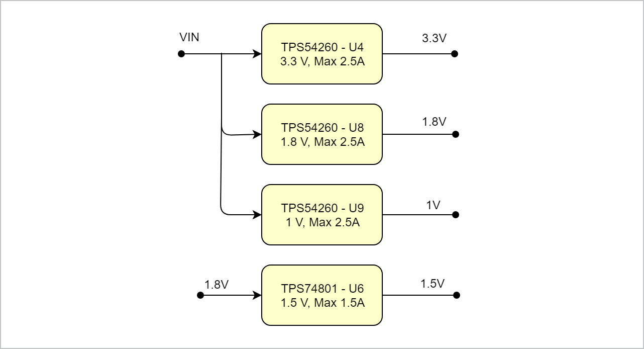
| title | Power Dependencies |
|---|
|
| Scroll Ignore |
|---|
| draw.io Diagram |
|---|
| border | false |
|---|
| viewerToolbar | true |
|---|
| |
|---|
| fitWindow | false |
|---|
| diagramDisplayName | |
|---|
| lbox | false |
|---|
| revision | 56 |
|---|
| diagramName | TE7028_PWR_PD |
|---|
| simpleViewer | false |
|---|
| width | |
|---|
| links | auto |
|---|
| tbstyle | hidden |
|---|
| diagramWidth | 641 |
|---|
|
|
| Scroll Only |
|---|
|
|
...
| Scroll Title |
|---|
| anchor | Figure_PWR_PS |
|---|
| title | Power On Sequence |
|---|
|
| Scroll Ignore |
|---|
| scroll-pdf | true |
|---|
| scroll-office | true |
|---|
| scroll-chm | true |
|---|
| scroll-docbook | true |
|---|
| scroll-eclipsehelp | true |
|---|
| scroll-epub | true |
|---|
| scroll-html | true |
|---|
| | draw.io Diagram |
|---|
| border | false |
|---|
| viewerToolbar | true |
|---|
| |
|---|
| fitWindow | false |
|---|
| diagramDisplayName | |
|---|
| lbox | true |
|---|
| revision | 23 |
|---|
| diagramName | TE0728_PWR_PS |
|---|
| simpleViewer | false |
|---|
| width | |
|---|
| links | auto |
|---|
| tbstyle | hidden |
|---|
| diagramWidth | 649 |
|---|
|
|
| Scroll Only |
|---|
| scroll-pdf | true |
|---|
| scroll-office | true |
|---|
| scroll-chm | true |
|---|
| scroll-docbook | true |
|---|
| scroll-eclipsehelp | true |
|---|
| scroll-epub | true |
|---|
| scroll-html | true |
|---|
| 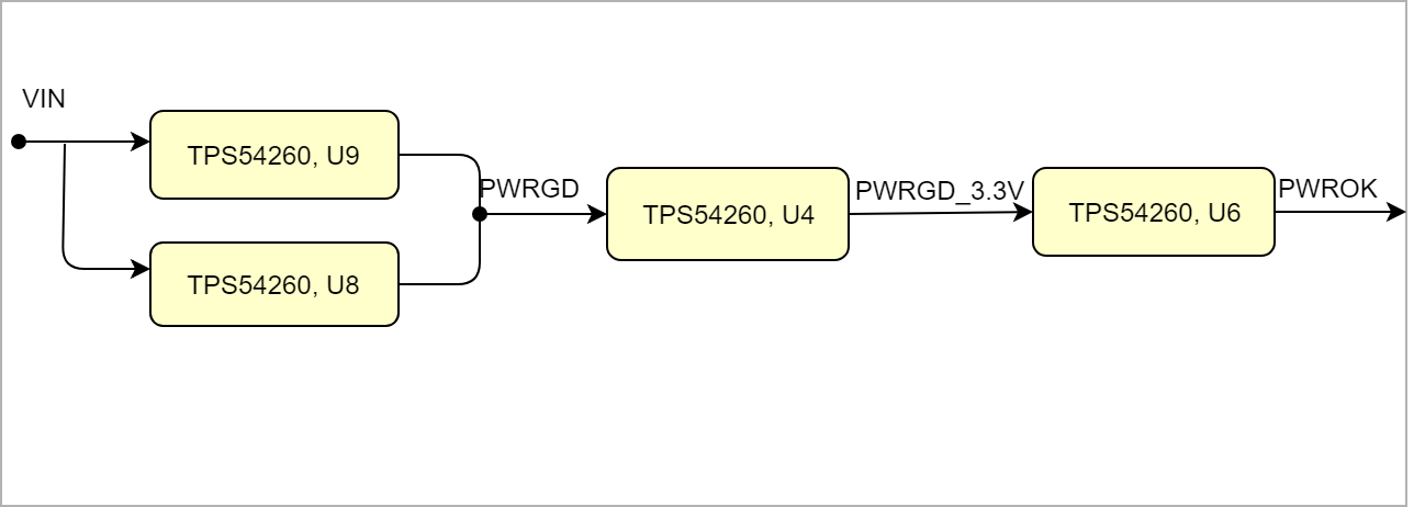 Image Modified Image Modified
|
|
Voltage Monitor Circuit
...
| Scroll Title |
|---|
| anchor | Table_TS_AMR |
|---|
| title | Absolute maximum ratings |
|---|
|
| Scroll Table Layout |
|---|
| orientation | portrait |
|---|
| sortDirection | ASC |
|---|
| repeatTableHeaders | default |
|---|
| style | |
|---|
| widths | |
|---|
| sortByColumn | 1 |
|---|
| sortEnabled | false |
|---|
| cellHighlighting | true |
|---|
|
| Symbols | Min | Max | Unit | Description | VCCO_DDR | -0.5 | 2.0 | V | PS DDR I/O supply voltage |
|---|
| VCCO_MIO0 | -0.5 | 3.6 | V | PS MIO I/O supply voltage for HR I/O banks | | VCCO_MIO1 | 1.71 | 3.45 | V | PS MIO I/O supply voltage for HR I/O banks | | VCCO | -0.5 | 3.6 | V | PL supply voltage for HR I/O banks | | VIN | 1.71 | 3.45 | V | I/O input voltage for HR I/O banks |
|
...
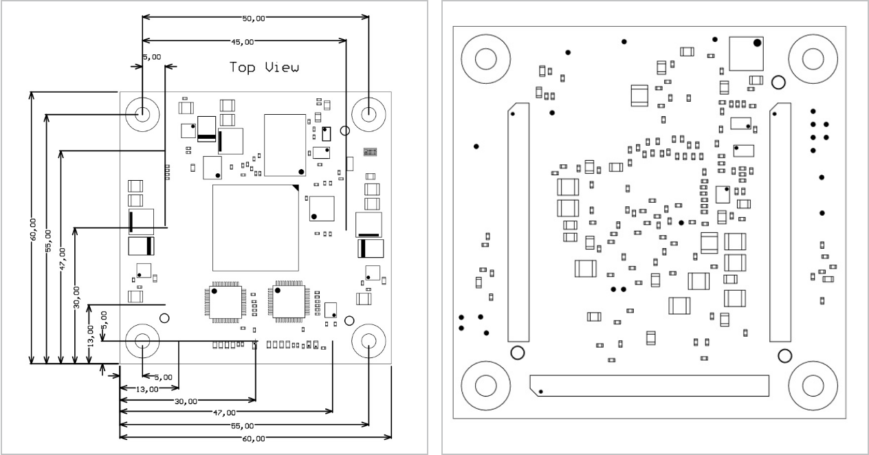
| Scroll Title |
|---|
| anchor | Figure_TS_PD |
|---|
| title | Physical Dimension |
|---|
|
| Scroll Ignore |
|---|
| draw.io Diagram |
|---|
| border | false |
|---|
| viewerToolbar | true |
|---|
| |
|---|
| fitWindow | false |
|---|
| diagramDisplayName | |
|---|
| lbox | false |
|---|
| revision | 22 |
|---|
| diagramName | TE0728_MC1 |
|---|
| simpleViewer | true |
|---|
| width | |
|---|
| links | auto |
|---|
| tbstyle | hidden |
|---|
| diagramWidth | 632 |
|---|
|
|
| Scroll Only |
|---|
| scroll-pdf | true |
|---|
| scroll-office | true |
|---|
| scroll-chm | true |
|---|
| scroll-docbook | true |
|---|
| scroll-eclipsehelp | true |
|---|
| scroll-epub | true |
|---|
| scroll-html | true |
|---|
| 
|
|
...
Current Offered Variants
...
| draw.io Diagram |
|---|
| border | false |
|---|
| viewerToolbar | true |
|---|
| |
|---|
| fitWindow | false |
|---|
| diagramDisplayName | |
|---|
| lbox | true |
|---|
| revision | 1619 |
|---|
| diagramName | TE0728_OV_BD |
|---|
| simpleViewer | false |
|---|
| width | |
|---|
| links | auto |
|---|
| tbstyle | hidden |
|---|
| diagramWidth | 641 |
|---|
|