...
| Scroll Title |
|---|
| anchor | Table_SIP_B2B |
|---|
| title | General overview of PL I/O signals and SoM's interfaces connected to the B2B connectors |
|---|
|
| Scroll Table Layout |
|---|
| orientation | portrait |
|---|
| sortDirection | ASC |
|---|
| repeatTableHeaders | default |
|---|
| style | |
|---|
| widths | |
|---|
| sortByColumn | 1 |
|---|
| sortEnabled | false |
|---|
| cellHighlighting | true |
|---|
|
| B2B Connector | Interfaces | I/O Signal Count | Notes |
|---|
| J1 | User IO | 72 single ended or 36 differential | 9x Pmod | | 6 LED | red | | 2 Push Button | - | | 7 MIO | J7 (not assembled), TE0724: 3.3V | | 2 MIO | J9 (not assembled), TE0724: 1.8V | | 1 MIO LED | green | | 1 MIO Push Button | - | | I²C | 2 | 1x Pmod | | SD IO | 7 | - | | UART | 2 | - | | CAN | 2 | - | | GbE PHY_MDIO + PHY_LEDs | 10 | - | | JTAG | 4 | - | | Power GPIO | 2 | - | | Power/Reset/Fuse programming | 3 | - | | Bootmode | 2 | - |
|
microUSB JTAG/UART Interface
There is no device with JTAG port on the baseboard. The microUSB connector provides JTAG access to the module is provided through B2B connector J1. This is routed to the carriers USB to JTAG/UART bridge, routed to B2B connector J1. The UART is routed via a levelshifter. There is no device with JTAG port on the baseboard.
| Scroll Title |
|---|
| anchor | Table_SIP_JTG |
|---|
| title | JTAG pins connection |
|---|
|
| Scroll Table Layout |
|---|
| orientation | portrait |
|---|
| sortDirection | ASC |
|---|
| repeatTableHeaders | default |
|---|
| style | |
|---|
| widths | |
|---|
| sortByColumn | 1 |
|---|
| sortEnabled | false |
|---|
| cellHighlighting | true |
|---|
|
JTAG Signal | B2B Connector Pin |
|---|
| TCK | J1-147 | | TDI | J1-151 | | TDO | J1-145 | | TMS | J1-149 | | UART RX | J1-36 | | UART TX | J1-38 |
|
SD Card Interface
| Scroll Title |
|---|
| anchor | Table_SIP_SDC |
|---|
| title | SD Card interface signals and connections |
|---|
|
| Scroll Table Layout |
|---|
| orientation | portrait |
|---|
| sortDirection | ASC |
|---|
| repeatTableHeaders | default |
|---|
| style | |
|---|
| widths | |
|---|
| sortByColumn | 1 |
|---|
| sortEnabled | false |
|---|
| cellHighlighting | true |
|---|
|
| Connected To | Signal Name | Notes |
|---|
| J1-34 | SD-CD | Card detect switch, pulled up, low if card inserted. | | J1-24 | SD-D0 |
| | J1-22 | SD-CMD |
| | J1-20 | SD-CCLK |
| | J1-26 | SD-D1 |
| | J1-28 | SD-D2 |
| | J1-30 | SD-D3 |
|
|
...
There are no I2C devices on the base board. Pullup resistors have to be provided by the module.
On-board Peripherals
| HTML |
|---|
<!--
Components on the Module, like Flash, PLL, PHY...
--> |
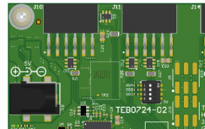
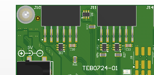
Pmods
Pmods
The GPIOs of the 10 Pmods (J10 The GPIOs of the 10 Pmods (J10 to J17, J20, J21) are connected with 100 Ohm differential routing to the B2B connector. J21 is a pure I2C compatible Pmod, without additional signals. The other 9 are GPIO Pmods where despite J20 all others can be used as dual Pmods.
...
| Scroll Title |
|---|
| anchor | Table_OBP_PMD |
|---|
| title | Pmod connections. |
|---|
|
| Scroll Table Layout |
|---|
| orientation | portrait |
|---|
| sortDirection | ASC |
|---|
| repeatTableHeaders | default |
|---|
| style | |
|---|
| widths | |
|---|
| sortByColumn | 1 |
|---|
| sortEnabled | false |
|---|
| cellHighlighting | true |
|---|
|
| J10 | J11 | J12 | J13 | J14 |
|---|
| PIN | Signal | B2B | Signal | B2B | Signal | B2B | Signal | B2B | Signal | B2B |
|---|
| 1 | PA0_P | J1-56 | PB2_N | J1-70 | PC2_P | J1-57 | PD2_P | J1-77 | PE2_N | J1-90 | | 2 | PA0_N | J1-58 | PB2_P | J1-72 | PC2_N | J1-55 | PD2_N | J1-75 | PE2_P | J1-92 | | 3 | PA3_P | J1-46 | PB0_N | J1-76 | PC0_P | J1-51 | PD0_P | J1-71 | PE0_N | J1-96 | | 4 | PA3_N | J1-48 | PB0_P | J1-78 | PC0_N | J1-49 | PD0_N | J1-69 | PE0_P | J1-98 | | 5 | GND | - | GND | - | GND | - | GND | - | GND | - | | 6 | VCCIO_35 | J1-54 | VCCIO_35 | J1-54 | VCCIO_35 | J1-54 | VCCIO_35 | J1-54 | VCCIO_35 | J1-54 | | 7 | PA1_N | J1-62 | PB3_P | J1-68 | PC3_N | J1-59 | PD3_N | J1-79 | PE3_P | J1-88 | | 8 | PA1_P | J1-60 | PB3_N | J1-66 | PC3_P | J1-61 | PD3_P | J1-81 | PE3_N | J1-86 | | 9 | PA2_N | J1-52 | PB1_P | J1-82 | PC1_N | J1-45 | PD1_N | J1-65 | PE1_P | J1-102 | | 10 | PA2_P | J1-50 | PB1_N | J1-80 | PC1_P | J1-47 | PD1_P | J1-67 | PE1_N | J1-100 | | 11 | GND | - | GND | - | GND | - | GND | - | GND | - | | 12 | B_VCCIO_35 | J1-54 | B_VCCIO_35 | J1-54 | B_VCCIO_35 | J1-54 | B_VCCIO_35 | J1-54 | B_VCCIO_35 | J1-54 |
| J15 | J16 | J17 | J20 | J21 |
|---|
| PIN | Signal | B2B | Signal | B2B | Signal | B2B | Signal | B2B | Signal | B2B |
|---|
| 1 | PG2_N | J1-110 | PF2_P | J1-97 | PH2_P | J1-115 | PI2_P | J1-133 | NC | - | | 2 | PG2_P | J1-112 | PF2_N | J1-95 | PH2_N | J1-113 | PI2_N | J1-131 | NC | - | | 3 | PG0_P | J1-114 | PF0_P | J1-91 | PH0_P | J1-111 | PI0_P | J1-129 | I2C_SCL | J1-142 | | 4 | PG0_N | J1-116 | PF0_N | J1-89 | PH0_N | J1-109 | PI0_N | J1-127 | I2C_SDA | J1-144 | | 5 | GND | - | GND | - | GND | - | GND | - | GND | - | | 6 | 3.3V | J1-74, J1- 43 | VCCIO_35 | J1-54 | 3.3V | J1-74, J1- 43 | 3.3V | J1-74, J1- 43 | 3.3V | J1-74, J1- 43 | | 7 | PG3_P | J1-108 | PF3_N | J1-99 | PH3_N | J1-117 | PI3_N | J1-135 | NC | - | | 8 | PG3_N | J1-106 | PF3_P | J1-101 | PH3_P | J1-119 | PI3_P | J1-137 | NC | - | | 9 | PG1_N | J1-120 | PF1_N | J1-85 | PH1_N | J1-105 | PI1_N | J1-123 | I2C_SCL | J1-142 | | 10 | PG1_P | J1-121 | PF1_P | J1-87 | PH1_P | J1-107 | PI1_P | J1-125 | I2C_SDA | J1-144 | | 11 | GND | - | GND | - | GND | - | GND | - | GND | - | | 12 | 3.3V | J1-74, J1- 43 | B_VCCIO_35 | J1-54 | 3.3V | J1-74, J1- 43 | 3.3V | J1-74, J1- 43 | 3.3V | J1-74, J1- 43 |
|
USB to JTAG/UART bridge
The TEB0724 carrier board has on-board microUSB 2.0 (J4) high-speed to UART/FIFO IC FT2232H (U1) from FTDI. Channel A can be used as JTAG Interface (MPSSE) to program on module JTAG devices. Channel B can be used as UART Interface routed via a level shifter to the 1.8V section of the B2B connector, usually connected to the PS of the SoM. There is also a 256-byte serial EEPROM connected to the FT2232H chip pre-programmed with license code to support Xilinx programming tools.
| Warning |
|---|
Do not access the FT2232H EEPROM using FTDI programming tools, doing so will erase normally invisible user EEPROM content and invalidate stored Xilinx JTAG license. Without this license the on-board JTAG will not be accessible any more with any Xilinx tools. Software tools from FTDI website do not warn or ask for confirmation before erasing user EEPROM content. |
CAN Screw Terminal
CAN Screw Terminal
The CAN bus is routed to screw terminal J2.
| Scroll Title |
|---|
| anchor | Table_OBP_CAN |
|---|
| title | CAN bus connection |
|---|
|
| Scroll Table Layout |
|---|
| orientation | portrait |
|---|
| sortDirection | ASC |
|---|
| repeatTableHeaders | default |
|---|
| style | |
|---|
| widths | |
|---|
| sortByColumn | 1 |
|---|
| sortEnabled | false |
|---|
| cellHighlighting | true |
|---|
|
| PIN | Signal | B2B |
|---|
| J2-1 | CAN0_N | J1-1 | | J2-2 | GND |
| | J2-3 | CAN0_P | J1-3 |
|
Jumpers on J22-1 to J22-3 and J22-2 to J22-4 connect proper split termination resistors to the CAN bus.
Pin Header J6 provides access to power functions, bootmode selection and PMIC In-Circuit Programming (For initial PMIC In-Circuit Programming of the module, Diode D28 has to be removed)The CAN bus is routed to screw terminal J2.
| Scroll Title |
|---|
| anchor | Table_OBP_CANPHJ6 |
|---|
| title | CAN bus connectionPin Header J6 |
|---|
|
| Scroll Table Layout |
|---|
| orientation | portrait |
|---|
| sortDirection | ASC |
|---|
| repeatTableHeaders | default |
|---|
| style | |
|---|
| widths | |
|---|
| sortByColumn | 1 |
|---|
| sortEnabled | false |
|---|
| cellHighlighting | true |
|---|
|
| PIN | Signal | B2B |
|---|
| J2-1 | CAN0_N | J1-1 | J2-2 | GND | | J2-3 | CAN0_P | J1-3 |
|
Jumpers on J22-1 to J22-3 and J22-2 to J22-4 connect proper split termination resistors to the CAN bus.
Oscillators
The module has the following reference clock signals provided by on-board oscillators:
...
| anchor | Table_OBP_CLK |
|---|
| title | Reference clock signals |
|---|
|
|---|
| J6-1 | VIN | J1-154, J1-156, J1-158, J1-160 | | J6-2 | VIN | J1-154, J1-156, J1-158, J1-160 | | J6-3 | GND |
| | J6-4 | GND |
| | J6-5 | I2C_SCL | J1-142 | | J6-6 | VBAT | J1-152 | | J6-7 | I2C_SDA | J1-144 | | J6-8 | PWR_GPIO2 | J1-143 | | J6-9 | ONKEY | J1-148 | | J6-10 | PWR_GPIO4 | J1-141 | | J6-11 | PWR_TP | J1-146 | | J6-12 | RESETREQ | J1-150 | | J6-13 | MODE0 | J1-2 | | J6-14 | GND |
| | J6-15 | MODE1 | J1-4 | | J6-16 | GND |
|
|
Alternatively to selecting B_VCCIO_35 by using S6 dip switches, VCCIO_35 ( e.g. SoM TE0724, Bank 35) can be selected by removing R45 and adding a jumper on optional J19. In table 18 valid jumper positions are given. Voltages and maximum current ratings could be found in the corresponding TRM of the attached module, (e.g. TE0724 TRM#PowerRails ).
...
| Scroll Title |
|---|
| anchor | Table_OBP_LEDPHJ19 |
|---|
| title | On-board LEDsOptional Pin Header J19 |
|---|
|
| Scroll Table Layout |
|---|
| orientation | portrait |
|---|
| sortDirection | ASC |
|---|
| repeatTableHeaders | default |
|---|
| style | |
|---|
| widths | |
|---|
| sortByColumn | 1 |
|---|
| sortEnabled | false |
|---|
| cellHighlighting | true |
|---|
|
|
| LED | Color | Signal | Description and Notes |
|---|
| D1 | green | VIN | power indicator |
| D2-D7 | red | ULED1..6 | User LED |
| D8 | green | MIO9 | MIO user LED |
| J3B | green | PHY_LED0 | Ethernet status |
| J3C | yellow | PHY_LED1 | Ethernet status |
...
| PIN | Signal | B2B |
|---|
| J19-1 | VLDO1 | J1-83 | | J19-2 | GND |
| | J19-3 | VCCIO_35 | J1-54 | | J19-4 | VLDO2 | J1-94 | J19-5 | VLDO34 | J1-53 | | J19-6 | GND |
|
|
| Scroll Title |
|---|
| anchor | Table_OBP_PBVSJ19 |
|---|
| title | On-board Push ButtonJ19 Jumper settings for VCCIO_35 voltage selection |
|---|
|
| Scroll Table Layout |
|---|
| orientation | portrait |
|---|
| sortDirection | ASC |
|---|
| repeatTableHeaders | default |
|---|
| style | |
|---|
| widths | |
|---|
| sortByColumn | 1 |
|---|
| sortEnabled | false |
|---|
| cellHighlighting | true |
|---|
|
|
| Button | Signal | B2B | Description and Notes |
|---|
| S1 | ONKEY | J1-148 | Power Button, pulled up, on push de-asserted |
| S3 | RESETREQ | J1-150 | User LED pulled up, on push de-asserted |
S2 | S2 | J1-124 | PL user button, pulled up, on push de-asserted |
| S4 | S4 | J1-126 | PL user button, pulled up, on push de-asserted |
| S5 | MIO51 | J1-42 | PS MIO user button, pulled up, on push de-asserted |
Dip-Switches
Dip-switch S6-1..3 are used to select the adjustable board power. Tabel 14 shows the signals, table 15 how to adjust the switches for corresponding B_VCCIO_35 Voltages.
...
| anchor | Table_OBP_DIS |
|---|
| title | Dip-Switches |
|---|
...
S6-3
...
| Jumper position | Signal | e.g. TE0724 |
|---|
| draw.io Diagram |
|---|
| border | false |
|---|
| viewerToolbar | true |
|---|
| |
|---|
| fitWindow | false |
|---|
| diagramDisplayName | |
|---|
| lbox | true |
|---|
| revision | 3 |
|---|
| diagramName | Jumper_Settings_J19_5-3_TEB0724 |
|---|
| simpleViewer | true |
|---|
| width | 200 |
|---|
| links | auto |
|---|
| tbstyle | top |
|---|
| diagramWidth | 293 |
|---|
|
|
J19 1-3 |
VLDO1 |
3.3V | | draw.io Diagram |
|---|
| border | false |
|---|
| viewerToolbar | true |
|---|
| |
|---|
| fitWindow | false |
|---|
| diagramDisplayName | |
|---|
| lbox | true |
|---|
| revision | 5 |
|---|
| diagramName | Jumper_Settings_J19_TEB0724 |
|---|
| simpleViewer | true |
|---|
| width | 200 |
|---|
| links | auto |
|---|
| tbstyle | top |
|---|
| diagramWidth | 293 |
|---|
|
|
J19 4-3 |
VLDO2 |
1,8V | | draw.io Diagram |
|---|
| border | false |
|---|
| viewerToolbar | true |
|---|
| |
|---|
| fitWindow | false |
|---|
| diagramDisplayName | |
|---|
| lbox | true |
|---|
| revision | 3 |
|---|
| diagramName | Jumper_Settings_J19_4-3_TEB0724 |
|---|
| simpleViewer | true |
|---|
| width | 200 |
|---|
| links | auto |
|---|
| tbstyle | top |
|---|
| diagramWidth | 293 |
|---|
|
|
J19 5-3 |
VLDO34 |
2,5V |
|
| Warning |
|---|
Respect VLDO current limitations!
|
Optional fitted headers J7, J8 and J9 are to provide full access to the Pins at the B2B connector, especially for testing and extension purposes. Description follows below.
PL Button and LED IOs are additionally routed to optionally assembled pin header J8.
...
| Scroll Title |
|---|
| anchor | Table_OBP_DSSPHJ8 |
|---|
| title | Select B_VCCIO_35 via Dip-Switches.Optional Pin Header J8 |
|---|
|
| Scroll Table Layout |
|---|
| orientation | portrait |
|---|
| sortDirection | ASC |
|---|
| repeatTableHeaders | default |
|---|
| style | |
|---|
| widths | |
|---|
| sortByColumn | 1 |
|---|
| sortEnabled | false |
|---|
| cellHighlighting | true |
|---|
|
| PIN | Signal | B2B |
|---|
| J8-1 | B_VCCIO_35 | S6-1 | S6-2 | S6-3 | 3.3V | ON | ON | ON |
|---|
| 2.5V | OFF | ON | ON | 1.8V | ON | OFF | ON | | 1.5V | OFF | OFF | ON | | 1.25V | ON | ON | OFF | | 1.2V | OFF | ON | OFF |
|
| J1-43, J1-74 | | J8-2 | GND |
| | J8-3 | S4 | J1-126 | | J8-4 | S2 | J1-124 | | J8-5 | ULED5 | J1-130 | | J8-6 | ULED6 | J1-128 | | J8-7 | ULED3 | J1-134 | | J8-8 | ULED4 | J1-132 | | J8-9 | ULED1 | J1-138 | | J8-10 | ULED2 | J1-136 |
|
Optional pin header J7 gives access to otherwise not used PS MIO IOs at a 3.3V bankPin Header J6 provides access to power functions, bootmode selection and PMIC In-Circuit Programming (For initial PMIC In-Circuit Programming of the module, Diode D28 has to be removed).
| Scroll Title |
|---|
| anchor | Table_OBP_PHJ6PHJ7 |
|---|
| title | Optional Pin Header J6J7 |
|---|
|
| Scroll Table Layout |
|---|
| orientation | portrait |
|---|
| sortDirection | ASC |
|---|
| repeatTableHeaders | default |
|---|
| style | |
|---|
| widths | |
|---|
| sortByColumn | 1 |
|---|
| sortEnabled | false |
|---|
| cellHighlighting | true |
|---|
|
| PIN | Signal | B2B |
|---|
| J6-1 | VIN | J1-154, J1-156, J1-158, J1-160 | | J6-2 | VIN | J1-154, J1-156, J1-158, J1-160 | J6-3 | GND | J6-4 | GND | | J6-5 | I2C_SCL | J1-142 | | J6-6 | VBAT | J1-152 | | J6-7 | I2C_SDA | J1-144 | | J6-8 | PWR_GPIO2 | J1-143 | | J6-9 | ONKEY | J1-148 | | J6-10 | PWR_GPIO4 | J1-141 | | J6-11 | PWR_TP | J1-146 | | J6-12 | RESETREQ | J1-150 | | J6-13 | MODE0 | J1-2 | J6-14 | GND | | J6-15 | MODE1 | J1-4 | J6-16 | GND | | B2B |
|---|
| J7-1 | 3.3V | 43, 74 | | J7-2 | GND |
| | J7-3 | GND |
| | J7-4 | MIO8 | J1-14 | | J7-5 | MIO10 | J1-31 | | J7-6 | MIO11 | J1-33 | | J7-7 | MIO12 | J1-35 | | J7-8 | MIO13 | J1-37 | | J7-9 | MIO14 | J1-39 | | J7-10 | MIO15 | J1-41 |
|
Optional pin header J9 gives access to otherwise not used PS MIO IOs at a 1.8V bankAlternatively to selecting B_VCCIO_35 by using S6 dip switches, VCCIO_35 ( e.g. SoM TE0724, Bank 35) can be selected by removing R45 and adding a jumper on optional J19. In table 18 valid jumper positions are given. Voltages and maximum current ratings could be found in the corresponding TRM of the attached module, (e.g. TE0724 TRM#PowerRails ).
| Scroll Title |
|---|
| anchor | Table_OBP_PHJ19PHJ9 |
|---|
| title | Optional Pin Header J19J9. |
|---|
|
| Scroll Table Layout |
|---|
| orientation | portrait |
|---|
| sortDirection | ASC |
|---|
| repeatTableHeaders | default |
|---|
| style | |
|---|
| widths | |
|---|
| sortByColumn | 1 |
|---|
| sortEnabled | false |
|---|
| cellHighlighting | true |
|---|
|
| PIN | Signal | B2B |
|---|
| J19J9-1 | VLDO11.8V | J1-8363 | | J19J9-2 | GND |
| | J9-3 | GND |
| | J9-4 | MIO_46 | J1-32 | | J9-5 | MIO_50 | J1-40 | | J9-6 | MIO_PB | J19-3 | VCCIO_35 | J1- 5442 J19 |
|
On-
...
board Peripherals
...
J19-5
...
| anchor | Table_OBP_VSJ19 |
|---|
| title | J19 Jumper settings for VCCIO_35 voltage selection |
|---|
...
J19 1-3
VLDO1
3.3V
...
J19 4-3
VLDO2
1,8V
...
J19 5-3
VLDO34
2,5V
| Warning |
|---|
Respect VLDO current limitations!
|
Optional fitted headers J7, J8 and J9 are to provide full access to the Pins at the B2B connector, especially for testing and extension purposes. Description follows below.
...
| HTML |
|---|
<!--
Components on the Module, like Flash, PLL, PHY...
--> |
USB to JTAG/UART bridge
The TEB0724 carrier board has on-board microUSB 2.0 (J4) high-speed to UART/FIFO IC FT2232H (U1) from FTDI. Channel A can be used as JTAG Interface (MPSSE) to program on module JTAG devices. Channel B can be used as UART Interface routed via a level shifter to the 1.8V section of the B2B connector, usually connected to the PS of the SoM. There is also a 256-byte serial EEPROM connected to the FT2232H chip pre-programmed with license code to support Xilinx programming tools.
| Warning |
|---|
Do not access the FT2232H EEPROM using FTDI programming tools, doing so will erase normally invisible user EEPROM content and invalidate stored Xilinx JTAG license. Without this license the on-board JTAG will not be accessible any more with any Xilinx tools. Software tools from FTDI website do not warn or ask for confirmation before erasing user EEPROM content. |
Oscillators
The module has the following reference clock signals provided by on-board oscillators:
| Scroll Title |
|---|
| anchor | Table_OBP_CLK |
|---|
| title | Reference clock signals |
|---|
|
| Scroll Table Layout |
|---|
| orientation | portrait |
|---|
| sortDirection | ASC |
|---|
| repeatTableHeaders | default |
|---|
| style | |
|---|
| widths | |
|---|
| sortByColumn | 1 |
|---|
| sortEnabled | false |
|---|
| cellHighlighting | true |
|---|
|
| Clock Source | Schematic Name | Frequency | Clock Destination |
|---|
| SiTime SiT8008AI oscillator, U4 | OSCI | 12.000000 MHz | U1, pin 3. |
|
On-board LEDs
| Scroll Title |
|---|
| anchor | Table_OBP_LED |
|---|
| title | On-board LEDs |
|---|
|
| Scroll Table Layout |
|---|
| orientation | portrait |
|---|
| sortDirection | ASC |
|---|
| repeatTableHeaders | default |
|---|
| style | |
|---|
| widths | |
|---|
| sortByColumn | 1 |
|---|
| sortEnabled | false |
|---|
| cellHighlighting | true |
|---|
|
| LED | Color | Signal | Description and Notes |
|---|
| D1 | green | VIN | power indicator | | D2-D7 | red | ULED1..6 | User LED | | D8 | green | MIO9 | MIO user LED | | J3B | green | PHY_LED0 | Ethernet status | | J3C | yellow | PHY_LED1 | Ethernet status |
|
On-board Push Buttons
| Scroll Title |
|---|
| anchor | Table_OBP_PHJ8PB |
|---|
| title | Optional Pin Header J8On-board Push Button |
|---|
|
| Scroll Table Layout |
|---|
| orientation | portrait |
|---|
| sortDirection | ASC |
|---|
| repeatTableHeaders | default |
|---|
| style | |
|---|
| widths | |
|---|
| sortByColumn | 1 |
|---|
| sortEnabled | false |
|---|
| cellHighlighting | true |
|---|
|
| PINButton | Signal | B2B |
|---|
| J8-1 | 3.3V | J1-43, J1-74 | | Description and Notes |
|---|
| S1 | ONKEY | J8-2 | GND | J8-3 | S4 | J1- | 126 | J8-4 | S2 | J1-124 | | J8-5 | ULED5 | J1-130 | | J8-6 | ULED6 | J1-128 | | J8-7 | ULED3 | J1-134 | | J8-8 | ULED4 | J1-132 | | J8-9 | ULED1 | J1-138 | | J8-10 | ULED2 | J1-136 | | 148 | Power Button, pulled up, on push de-asserted | | S3 | RESETREQ | J1-150 | User LED pulled up, on push de-asserted | S2 | S2 | J1-124 | PL user button, pulled up, on push de-asserted | | S4 | S4 | J1-126 | PL user button, pulled up, on push de-asserted | | S5 | MIO51 | J1-42 | PS MIO user button, pulled up, on push de-asserted |
|
Dip-Switches
Dip-switch S6-1..3 are used to select the adjustable board power. Tabel 14 shows the signals, table 15 how to adjust the switches for corresponding B_VCCIO_35 VoltagesOptional pin header J7 gives access to otherwise not used PS MIO IOs at a 3.3V bank.
| Scroll Title |
|---|
| anchor | Table_OBP_PHJ7DIS |
|---|
| title | Optional Pin Header J7Dip-Switches |
|---|
|
| Scroll Table Layout |
|---|
| orientation | portrait |
|---|
| sortDirection | ASC |
|---|
| repeatTableHeaders | default |
|---|
style | widths | | sortByColumn | 1 |
|---|
| sortEnabled | false |
|---|
| cellHighlighting | true |
|---|
|
|
| PIN | Signal | B2B |
|---|
| J7-1 | 3.3V | 43, 74 |
J7-2 | GND | J7-3 | GND | | J7-4 | MIO8 | J1-14 |
| J7-5 | MIO10 | J1-31 |
| J7-6 | MIO11 | J1-33 |
| J7-7 | MIO12 | J1-35 |
| J7-8 | MIO13 | J1-37 |
| J7-9 | MIO14 | J1-39 |
| J7-10 | MIO15 | J1-41 |
...
| ASC |
|---|
| repeatTableHeaders | default |
|---|
| style | |
|---|
| widths | |
|---|
| sortByColumn | 1 |
|---|
| sortEnabled | false |
|---|
| cellHighlighting | true |
|---|
|
| Switch | Signal |
|---|
| S6-1 | VADJ_VS0 | | S6-2 | VADJ_VS1 | S6-3 | VADJ_VS2 | | S6-4 | NC |
|
| Scroll Title |
|---|
| anchor | Table_OBP_PHJ9DSS |
|---|
| title | Optional Pin Header J9Select B_VCCIO_35 via Dip-Switches. |
|---|
|
| Scroll Table Layout |
|---|
| orientation | portrait |
|---|
| sortDirection | ASC |
|---|
| repeatTableHeaders | default |
|---|
| style | |
|---|
| widths | |
|---|
| sortByColumn | 1 |
|---|
| sortEnabled | false |
|---|
| cellHighlighting | true |
|---|
|
| B_VCCIO_35 | S6-1 | S6-2 | S6-3 |
|---|
| 3.3V | ON | ON | ON | | 2.5V | OFF | ON | ON | | PIN | Signal | B2B |
|---|
| J9-1 | 1.8V | ON | J1-63 | J9-2 | GND | J9-3 | GND | | J9-4 | MIO_46 | J1-32 | | J9-5 | MIO_50 | J1-40 | | OFF | ON | | 1.5V | OFF | OFF | ON | | 1.25V | ON | ON | OFF | | 1.2V | OFF | ON | OFF | J9-6 | MIO_PB | J1-42 |
|
Power and Power-On Sequence
...
| Page properties |
|---|
|
- This section is optional and only for modules.
- use "include page" macro and link to the general B2B connector page of the module series, for example: 4 x 5 SoM LSHM B2B Connectors
|
| Include Page |
|---|
| PD:4 x 6 SoM SS5/ST5 B2B Connectors |
|---|
| PD:4 x 6 SoM SS5/ST5 B2B Connectors |
|---|
|
...
| Page properties |
|---|
|
In 'Physical Dimension' section, top and button view of moduloe must be insterted, information regarding physical dimention can be obtained through webpage for product in Shop.Trenz, (Download> Documents> Assembly part)for every SoM. For Example: for Module TE0728, Physical Dimension information can be captured by snipping tools from the link below: https://www.trenz-electronic.de/fileadmin/docs/Trenz_Electronic/Modules_and_Module_Carriers/5.2x7.6/TE0745/REV02/Documents/AD-TE0745-02-30-1I.PDF |
| Scroll Title |
|---|
| anchor | Figure_TS_PD |
|---|
| title | Physical Dimension |
|---|
|
 Image Removed Image Removed
Image Removed |
| Scroll Title |
|---|
| anchor | Figure_TS_PD |
|---|
| title | Physical Dimension |
|---|
|
| Scroll Title |
|---|
| anchor | Figure_TS_PD |
|---|
| title | Physical dimensions drawing |
|---|
|  Image Added Image Added| draw.io Diagram |
|---|
| border | false |
|---|
| viewerToolbar | true |
|---|
| |
|---|
| fitWindow | false |
|---|
| diagramDisplayName | |
|---|
| lbox | true |
|---|
| revision | 3 |
|---|
| diagramName | AD_TEB0724 |
|---|
| simpleViewer | true |
|---|
| width | |
|---|
| links | auto |
|---|
| tbstyle | top |
|---|
| diagramWidth | 641 |
|---|
|
 Image Added Image Added |
| Scroll Only |
|---|
| scroll-pdf | true |
|---|
| scroll-office | true |
|---|
| scroll-chm | true |
|---|
| scroll-docbook | true |
|---|
| scroll-eclipsehelp | true |
|---|
| scroll-epub | true |
|---|
| scroll-html | true |
|---|
|
|
|
Currently Offered Variants
...
Document Change History
...